基于AS8002设计的太阳能电源逆变技术
时间:06-12
来源:互联网
点击:
AS8002是太阳能电源逆变器高精度测量IC. 太阳能光伏系统(PV)中的电源逆变器常常直接连接到国家电网,注入电能,这些电能必须符合某种规范.AS8002中的12位100kSPS ADC能高精度地测量所监管的电压和电流,可编程增益放大器适合不同类型的传感器,片内的基准电压有很低的温度系数(10ppm/K). AS8002适用于PV逆变器电网监测,风能逆变器电网监测,隔离电压检测和UPS.本文介绍了AS8002主要特性,方框图, 典型应用电路图以及AS8002电源逆变器适配器板主要特性与电路图.
Power inverters in solar photovoltaic systems are often connected directly to the electricity grid in order to inject the created energy into the mains and act as an electricity supplier. This energy must comply with certain regulations that set the standard in terms of quality and safety which requires of accurate measurements.
The AS8002 is a highly accurate measurement IC that allows monitoring the generated energy with low cost shunt resistors or other sensors for the current and resistor dividers for the voltage.
This approach allows avoiding more expensive sensing devices while achieving the required accuracy for DC and AC measurements of current and voltage, as well as stability over the operating temperature range of the inverter.
The 12-bit ADC samples the voltage and current and provides their instantaneous values through an SPI interface.
The 12-bit ADC is preceded by low noise programmable gain amplifiers in order to accommodate different sensors.
The ADC has three multiplexed inputs, offering one secondary channel in addition to the main voltage and current.
The on-chip temperature sensor provides the inverter designer the option of temperature compensation for any of the measured parameters or functional blocks provided, over the full operating temperature range of the device.
The on-chip voltage reference is connected to the ADC and to REF. An external crystal oscillator is not required as a high accuracy internal oscillator clock is available.
The independent over current interrupt detects a high current on the grid and allows the processor to open the switches without waiting for the ADC conversion.
AS8002主要特性:
12-Bit 100 kSPS ADCs for accurate voltage and current measurement
Programmable gain amplifiers to accommodate for different sensors
Three multiplexed inputs to the 12-Bit ADC for secondary measurements that require high accuracy and fast sampling rates
On chip temperature sensor connected to one of the inputs of the multiplexer
On-chip voltage reference with small temperature coefficient (10ppm/K typ). This reference is available at the pin REF.
Low power on chip oscillator
SPI compatible interface
Internal registers for easy offset and gain compensation
Interrupt alerts (including Under Voltage Lock-Out and Over Temperature)
Independent programmable over current interrupt
AS8002应用:
The AS8002 is suitable for PV inverter grid monitoring, Wind inverter grid monitoring, Isolated voltage sensing, Uninterruptible Power supplies and Power conditioners.
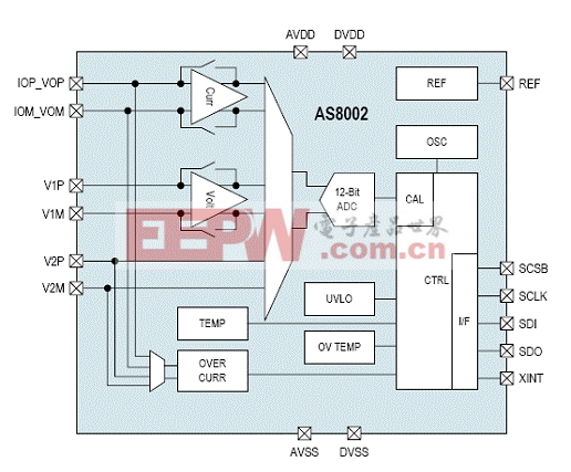
图1.AS8002方框图

图2.AS8002典型应用电路图
AS8002电源逆变器适配器板
Power inverters in solar photovoltaic systems are often connected directly to the electricity grid in order to inject the created energy into the mains and act as an electricity supplier. This energy must comply with certain regulations that set the standard in terms of quality and safety which requires of accurate measurements.
The AS8002 is a highly accurate measurement IC that allows monitoring the generated energy with low cost shunt resistors or other sensors for the current and resistor dividers for the voltage. This approach allows avoiding more expensive sensing devices while achieving the required accuracy for DC and AC measurements of current and voltage as well as stability over the operating temperature range of the inverter.
The 12 bit ADC samples the voltage and current and provides their instantaneous values through an SPI interface.
The 12 Bit ADC is preceded by low noise programmable gain amplifiers in order to accommodate different sensors. The ADC has three multiplexed inputs, offering one secondary channel in addition to the main voltage and current.
The on-chip temperature sensor provides the inverter designer the option of temperature compensation for any of the measured parameters or functional blocks provided, over the full operating temperature range of the device.
The on-chip voltage reference is connected to the ADC and to REF. An external crystal oscillator is not required as a high accuracy internal oscillator clock is available.
The independent over current interrupt detects a high current on the grid and allows the processor to open the switches without waiting for the ADC conversion.
The AS8002 Adapter Board
The AS8002-AB-1.0 Adapter board allows you an easy-to-use evaluation of the essential functions of the AS8002. It is a system with built-in microcontroller, USB interface and a simple analogue frontend. The complete system is fully supplied by the PC and needs no additional external power supply.
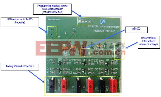
图3.AS8002电源逆变器适配器板外形图
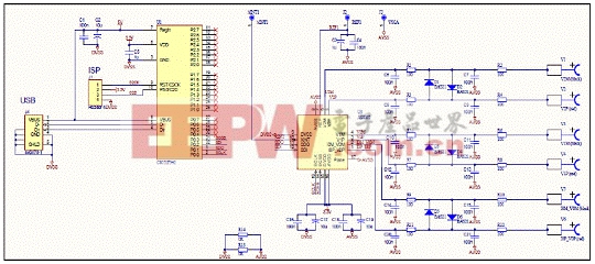
图4.AS8002适配器板电路图
Power inverters in solar photovoltaic systems are often connected directly to the electricity grid in order to inject the created energy into the mains and act as an electricity supplier. This energy must comply with certain regulations that set the standard in terms of quality and safety which requires of accurate measurements.
The AS8002 is a highly accurate measurement IC that allows monitoring the generated energy with low cost shunt resistors or other sensors for the current and resistor dividers for the voltage.
This approach allows avoiding more expensive sensing devices while achieving the required accuracy for DC and AC measurements of current and voltage, as well as stability over the operating temperature range of the inverter.
The 12-bit ADC samples the voltage and current and provides their instantaneous values through an SPI interface.
The 12-bit ADC is preceded by low noise programmable gain amplifiers in order to accommodate different sensors.
The ADC has three multiplexed inputs, offering one secondary channel in addition to the main voltage and current.
The on-chip temperature sensor provides the inverter designer the option of temperature compensation for any of the measured parameters or functional blocks provided, over the full operating temperature range of the device.
The on-chip voltage reference is connected to the ADC and to REF. An external crystal oscillator is not required as a high accuracy internal oscillator clock is available.
The independent over current interrupt detects a high current on the grid and allows the processor to open the switches without waiting for the ADC conversion.
AS8002主要特性:
12-Bit 100 kSPS ADCs for accurate voltage and current measurement
Programmable gain amplifiers to accommodate for different sensors
Three multiplexed inputs to the 12-Bit ADC for secondary measurements that require high accuracy and fast sampling rates
On chip temperature sensor connected to one of the inputs of the multiplexer
On-chip voltage reference with small temperature coefficient (10ppm/K typ). This reference is available at the pin REF.
Low power on chip oscillator
SPI compatible interface
Internal registers for easy offset and gain compensation
Interrupt alerts (including Under Voltage Lock-Out and Over Temperature)
Independent programmable over current interrupt
AS8002应用:
The AS8002 is suitable for PV inverter grid monitoring, Wind inverter grid monitoring, Isolated voltage sensing, Uninterruptible Power supplies and Power conditioners.

图1.AS8002方框图

图2.AS8002典型应用电路图
AS8002电源逆变器适配器板
Power inverters in solar photovoltaic systems are often connected directly to the electricity grid in order to inject the created energy into the mains and act as an electricity supplier. This energy must comply with certain regulations that set the standard in terms of quality and safety which requires of accurate measurements.
The AS8002 is a highly accurate measurement IC that allows monitoring the generated energy with low cost shunt resistors or other sensors for the current and resistor dividers for the voltage. This approach allows avoiding more expensive sensing devices while achieving the required accuracy for DC and AC measurements of current and voltage as well as stability over the operating temperature range of the inverter.
The 12 bit ADC samples the voltage and current and provides their instantaneous values through an SPI interface.
The 12 Bit ADC is preceded by low noise programmable gain amplifiers in order to accommodate different sensors. The ADC has three multiplexed inputs, offering one secondary channel in addition to the main voltage and current.
The on-chip temperature sensor provides the inverter designer the option of temperature compensation for any of the measured parameters or functional blocks provided, over the full operating temperature range of the device.
The on-chip voltage reference is connected to the ADC and to REF. An external crystal oscillator is not required as a high accuracy internal oscillator clock is available.
The independent over current interrupt detects a high current on the grid and allows the processor to open the switches without waiting for the ADC conversion.
The AS8002 Adapter Board
The AS8002-AB-1.0 Adapter board allows you an easy-to-use evaluation of the essential functions of the AS8002. It is a system with built-in microcontroller, USB interface and a simple analogue frontend. The complete system is fully supplied by the PC and needs no additional external power supply.

图3.AS8002电源逆变器适配器板外形图

图4.AS8002适配器板电路图
逆变 技术 电源 太阳能 AS8002 设计 基于 相关文章:
- 实现智能太阳能管理的微型逆变器应运而生(05-06)
- 只需少量器件的廉价自动复位断路器(07-31)
- 即将普及的碳化硅器件(10-19)
- IR2110驱动电路的优化设计(03-15)
- 关键电源及LED照明应用的最新高能效规范要求、设计挑战及解决方案(12-07)
- 基于FPGA的三相PWM发生器(06-23)
