ADIADM12752V-20V热插拔控制方案
时间:03-14
来源:互联网
点击:
ADI公司的ADM1275是2V-20V的热插拔控制器,能使电路板插入或拔出带电背板,控制电源电压为2V-20V,限流电阻可编程从5mV到25mV,12位ADC的精度为±1%,电荷泵栅极驱动器用来驱动多个外接N-沟FET,高栅极驱动电压保证了最低的RDSON,主要用在电源监视,电讯和数据通信设备,PC/服务器等.本文介绍了ADM1275主要特性,方框图,以及评估板EVAL-ADM127xEBZ主要特性,电路图,材料清单和PCB布局图.
The ADM1275 is a hot-swap controller that allows a circuit board to be removed from or inserted into a live backplane. It also features current and voltage readback via an integrated 12-bit analog-to-digital converter (ADC), accessed using a PMBus? interface.
The load current is measured using an internal current sense amplifier that measures the voltage across a sense resistor in the power path via the SENSE+ and SENSE? pins. A default limit of 20 mV is set, but this limit can be adjusted, if required, using a resistor divider network from the internal reference voltage to the ISET pin.
The ADM1275 limits the current through the sense resistor by controlling the gate voltage of an external N-channel FET in the power path, via the GATE pin. The sense voltage—and, therefore, the load current—is maintained below the preset maximum. The ADM1275 protects the external FET by limiting the time that the FET remains on while the current is at its maximum value. This current limit time is set by the choice of capacitor connected to the TIMER pin. In addition, a foldback resistor network can be used to actively lower the current limit as the voltage across the FET is increased. This helps to maintain constant power in the FET and allows the safe operating area (SOA) to be adhered to in an effective manner.
In case of a short-circuit event, a fast internal overcurrent detec-tor responds within 370 ns and signals the gate to shut down. A 1500 mA pull-down device ensures a fast FET response. The ADM1275 features overvoltage and undervoltage protection, programmed using external resistor dividers on the UV and OV pins. A PWRGD signal can be used to detect when the output supply is valid, using the FLB pin to monitor the output. GPO pins can be configured as various output signals that can be asserted when a programmed current or voltage level is reached.
The 12-bit ADC can measure the current in the sense resistor, as well as the supply voltage on the SENSE+ pin or the output voltage. A PMBus interface allows a controller to read current and voltage data from the ADC. Measurements can be initiated by a PMBus command. Alternatively, the ADC can run continu-ously, and the user can read the latest conversion data whenever required. Up to four unique PMBus addresses can be selected, depending on the way that the ADR pin is connected.
The ADM1275-1 and ADM1275-3 are available in a 20-lead QSOP and 20-lead LFCSP and have a LATCH pin that can be configured for automatic retry or latch-off when an overcurrent fault occurs. The ADM1275-2 is available in a 16-lead QSOP with latch-off mode only.
ADM1275主要特性:
Controls supply voltages from 2 V to 20 V
370 ns response time to short circuit
Resistor-programmable 5 mV to 25 mV current limit
±1% accurate, 12-bit ADC for current, VIN/VOUT readback
Charge-pumped gate drive for multiple external N-channel FETs
High gate drive voltage to ensure lowest RDSON
Foldback for tighter FET SOA protection
Automatic retry or latch-off on current fault
Programmable current limit timer for SOA
Programmable, multifunction GPOs
Power-good status output
Analog UV and OV protection
ENABLE pin (ADM1275-3 only)
Peak detect registers for current and voltage
PMBus fast mode compliant interface
16-lead QSOP and 20-lead QSOP and LFCSP
ADM1275应用:
Power monitoring and control/power budgeting
Central office equipment
Telecommunication and data communication equipment
PCs/servers

图1.ADM1275-1功能方框图
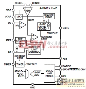
图2.ADM1275-2功能方框图
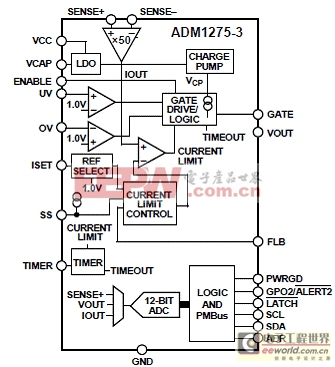
图3.ADM1275-3功能方框图
评估板EVAL-ADM127xEBZ
The EVAL-ADM127xEBZ is a compact full feature evaluation board for the ADM1275-1ACPZ, ADM1275-3ACPZ, and ADM1276-3ACPZ devices. The elaborated layout gives users a clear visual of all the peripheral components and the hot-swap power path. The layout also maximizes the board’s ability to dissipate heat for some of the key components on the power path, allowing the evaluation of very high current hot-swap setups.
Three sense-resistor slots and six multipackage FET slots give users great flexibility and allow them to simulate a wide range of application setups.
Multiple test points allow easy access to all critical points/pins. Six LEDs give users direct visual indication on variations in the board status, such as supply input, output, IC power good output, latch output, and GPO outputs. Six ADT75 digital temperature sensors on the back of the board allow users to obtain the board’s thermal data through an I2C bus in real time.
The kit supports I2C communication, allowing users to communicate with the ADM1275/ADM1276 and the ADT75. The evaluation kit also supports cascade setup so multiple evaluation boards can be connected together and share the same I2C bus.
The boards are fully compatible with the ADM1275/ADM1276 evaluation software tool, which can be downloaded at: www.analog.com/hotswap_powermonitor.
Note that users may need the USB-to-I2C dongle, USB-SMBUS-CABLEZ, to use the evaluation software tools.
The standard evaluation kit is prepopulated and tested with a 12 V, 60 A hot-swap design capable of working with a 4.7 mF output capacitor.
Complete specifications for the ADM1275 and the ADM1276 are available in the ADM1275 and the ADM1276 data sheets available from Analog Devices and should be consulted in conjunction with this user guide when using the evaluation boards.
评估板EVAL-ADM127xEBZ主要特性:
Full functions support evaluation kit for the ADM1275 and the ADM1276
Supports LFCSP device package
Populated and tested with 12 V, 60 A, 4.7 mF design
Capable of evaluating high current designs for over 100 A
Special NMOSFET footprint suits different packages
Supports up to 3 sense resistors in parallel
Supports up to 6 FETs in parallel
LED indicated status outputs
Wild input voltage range of up to 20 V
Allows separate VCC and VIN for low voltage sensing
6 on-board ADT75 accurate temperature sensors
Supports cascade setup for multiple boards
Toggle and push-button switch for easy input control
PMBus communication support
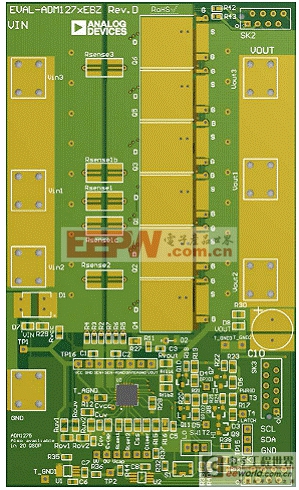
图4.评估板EVAL-ADM127xEBZ外形图
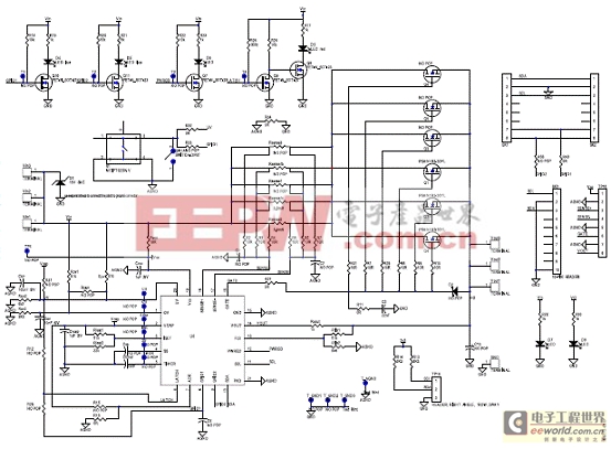
图5.评估板EVAL-ADM127xEBZ电路图(1)
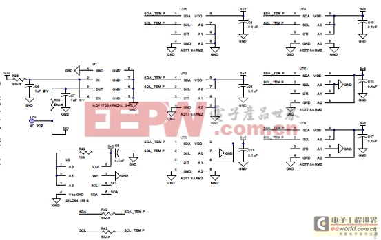
图6.评估板EVAL-ADM127xEBZ电路图(2)

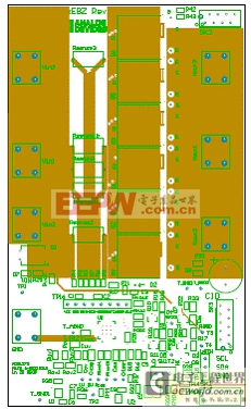
图7.评估板EVAL-ADM127xEBZ PCB布局图
评估板EVAL-ADM127xEBZ材料清单(BOM):

详情请见:
http://www.analog.com/static/imported-files/data_sheets/ADM1275.pdf
和
http://www.analog.com/static/imported-files/user_guides/UG-263.pdf
The ADM1275 is a hot-swap controller that allows a circuit board to be removed from or inserted into a live backplane. It also features current and voltage readback via an integrated 12-bit analog-to-digital converter (ADC), accessed using a PMBus? interface.
The load current is measured using an internal current sense amplifier that measures the voltage across a sense resistor in the power path via the SENSE+ and SENSE? pins. A default limit of 20 mV is set, but this limit can be adjusted, if required, using a resistor divider network from the internal reference voltage to the ISET pin.
The ADM1275 limits the current through the sense resistor by controlling the gate voltage of an external N-channel FET in the power path, via the GATE pin. The sense voltage—and, therefore, the load current—is maintained below the preset maximum. The ADM1275 protects the external FET by limiting the time that the FET remains on while the current is at its maximum value. This current limit time is set by the choice of capacitor connected to the TIMER pin. In addition, a foldback resistor network can be used to actively lower the current limit as the voltage across the FET is increased. This helps to maintain constant power in the FET and allows the safe operating area (SOA) to be adhered to in an effective manner.
In case of a short-circuit event, a fast internal overcurrent detec-tor responds within 370 ns and signals the gate to shut down. A 1500 mA pull-down device ensures a fast FET response. The ADM1275 features overvoltage and undervoltage protection, programmed using external resistor dividers on the UV and OV pins. A PWRGD signal can be used to detect when the output supply is valid, using the FLB pin to monitor the output. GPO pins can be configured as various output signals that can be asserted when a programmed current or voltage level is reached.
The 12-bit ADC can measure the current in the sense resistor, as well as the supply voltage on the SENSE+ pin or the output voltage. A PMBus interface allows a controller to read current and voltage data from the ADC. Measurements can be initiated by a PMBus command. Alternatively, the ADC can run continu-ously, and the user can read the latest conversion data whenever required. Up to four unique PMBus addresses can be selected, depending on the way that the ADR pin is connected.
The ADM1275-1 and ADM1275-3 are available in a 20-lead QSOP and 20-lead LFCSP and have a LATCH pin that can be configured for automatic retry or latch-off when an overcurrent fault occurs. The ADM1275-2 is available in a 16-lead QSOP with latch-off mode only.
ADM1275主要特性:
Controls supply voltages from 2 V to 20 V
370 ns response time to short circuit
Resistor-programmable 5 mV to 25 mV current limit
±1% accurate, 12-bit ADC for current, VIN/VOUT readback
Charge-pumped gate drive for multiple external N-channel FETs
High gate drive voltage to ensure lowest RDSON
Foldback for tighter FET SOA protection
Automatic retry or latch-off on current fault
Programmable current limit timer for SOA
Programmable, multifunction GPOs
Power-good status output
Analog UV and OV protection
ENABLE pin (ADM1275-3 only)
Peak detect registers for current and voltage
PMBus fast mode compliant interface
16-lead QSOP and 20-lead QSOP and LFCSP
ADM1275应用:
Power monitoring and control/power budgeting
Central office equipment
Telecommunication and data communication equipment
PCs/servers

图1.ADM1275-1功能方框图

图2.ADM1275-2功能方框图

图3.ADM1275-3功能方框图
评估板EVAL-ADM127xEBZ
The EVAL-ADM127xEBZ is a compact full feature evaluation board for the ADM1275-1ACPZ, ADM1275-3ACPZ, and ADM1276-3ACPZ devices. The elaborated layout gives users a clear visual of all the peripheral components and the hot-swap power path. The layout also maximizes the board’s ability to dissipate heat for some of the key components on the power path, allowing the evaluation of very high current hot-swap setups.
Three sense-resistor slots and six multipackage FET slots give users great flexibility and allow them to simulate a wide range of application setups.
Multiple test points allow easy access to all critical points/pins. Six LEDs give users direct visual indication on variations in the board status, such as supply input, output, IC power good output, latch output, and GPO outputs. Six ADT75 digital temperature sensors on the back of the board allow users to obtain the board’s thermal data through an I2C bus in real time.
The kit supports I2C communication, allowing users to communicate with the ADM1275/ADM1276 and the ADT75. The evaluation kit also supports cascade setup so multiple evaluation boards can be connected together and share the same I2C bus.
The boards are fully compatible with the ADM1275/ADM1276 evaluation software tool, which can be downloaded at: www.analog.com/hotswap_powermonitor.
Note that users may need the USB-to-I2C dongle, USB-SMBUS-CABLEZ, to use the evaluation software tools.
The standard evaluation kit is prepopulated and tested with a 12 V, 60 A hot-swap design capable of working with a 4.7 mF output capacitor.
Complete specifications for the ADM1275 and the ADM1276 are available in the ADM1275 and the ADM1276 data sheets available from Analog Devices and should be consulted in conjunction with this user guide when using the evaluation boards.
评估板EVAL-ADM127xEBZ主要特性:
Full functions support evaluation kit for the ADM1275 and the ADM1276
Supports LFCSP device package
Populated and tested with 12 V, 60 A, 4.7 mF design
Capable of evaluating high current designs for over 100 A
Special NMOSFET footprint suits different packages
Supports up to 3 sense resistors in parallel
Supports up to 6 FETs in parallel
LED indicated status outputs
Wild input voltage range of up to 20 V
Allows separate VCC and VIN for low voltage sensing
6 on-board ADT75 accurate temperature sensors
Supports cascade setup for multiple boards
Toggle and push-button switch for easy input control
PMBus communication support

图4.评估板EVAL-ADM127xEBZ外形图

图5.评估板EVAL-ADM127xEBZ电路图(1)

图6.评估板EVAL-ADM127xEBZ电路图(2)


图7.评估板EVAL-ADM127xEBZ PCB布局图
评估板EVAL-ADM127xEBZ材料清单(BOM):

详情请见:
http://www.analog.com/static/imported-files/data_sheets/ADM1275.pdf
和
http://www.analog.com/static/imported-files/user_guides/UG-263.pdf
- 电源设计小贴士 1:为您的电源选择正确的工作频率(12-25)
- 超低静态电流电源管理IC延长便携应用工作时间(04-14)
- 负载点降压稳压器及其稳定性检查方法(07-19)
- 高效地驱动LED(04-23)
- 电源SOC:或许好用的“疯狂”创意(07-24)
- 实现智能太阳能管理的微型逆变器应运而生(05-06)
