SDRAM不能连续读取?
SDRAM的配置用的是官方例程,开发板用的是ATSAMV71Q21,求交流,求指导!
SDRAM配置代码如下
void sdram_fullconfig(void)
{
Pin pinsSdram[] = {BOARD_SDRAM_PINS}; //configure corresponding pin.
volatile uint32_t i;
volatile uint8_t *pSdram = (uint8_t *) SDRAM_CS_ADDR; //SDRAM first address
/* Configure PIO */
PIO_Configure(pinsSdram, PIO_LISTSIZE(pinsSdram));
PMC_EnablePeripheral(ID_SDRAMC);
MATRIX->CCFG_SMCNFCS = CCFG_SMCNFCS_SDRAMEN; //Enable the SDRAM support
/* 1. SDRAM features must be set in the configuration register:
asynchronous timings (TRC, TRAS, etc.), number of columns, rows,
CAS latency, and the data bus width. */
SDRAMC->SDRAMC_CR =
SDRAMC_CR_NC_COL8 // 8 column bits ,reset 8 column
| SDRAMC_CR_NR_ROW11 // 12 row bits (4K) ,reset 11 row
| SDRAMC_CR_CAS_LATENCY3 // CAS Latency 3 ,reset 2
| SDRAMC_CR_NB_BANK2 // 2 banks ,reset 2 bank
| SDRAMC_CR_DBW // 16 bit , reset 16
| SDRAMC_CR_TWR(5) //write recovery delay , reset 2
| SDRAMC_CR_TRC_TRFC(13) // 63ns min , row cycle delay and row refresh cycle delay ,reset 7
| SDRAMC_CR_TRP(5) // Command period (PRE to ACT) 21 ns min,reset 3
| SDRAMC_CR_TRCD(5) // Active Command to read/Write Command delay time 21ns min,reset 2
| SDRAMC_CR_TRAS(9) // Command period (ACT to PRE) 42ns min,reset 5
| SDRAMC_CR_TXSR(15U); // Exit self-refresh to active time 70ns Min ,reset 8
/* 2. For mobile SDRAM, temperature-compensated self refresh (TCSR), drive
strength (DS) and partial array self refresh (PASR) must be set in the
Low Power Register. */
/* 3. The SDRAM memory type must be set in the Memory Device Register.*/
SDRAMC->SDRAMC_MDR = SDRAMC_MDR_MD_SDRAM; //SDRAM or low power SDRAM
/* 4. A minimum pause of 200 μs is provided to precede any signal toggle.*/
for (i = 0; i < 100000; i++);
/* 5. (1)A NOP command is issued to the SDRAM devices. The application must
set Mode to 1 in the Mode Register and perform a write access to
any SDRAM address.*/
SDRAMC->SDRAMC_MR = SDRAMC_MR_MODE_NOP;
*pSdram = 0; //enable SDRAM
for (i = 0; i < 100000; i++);
/* 6. An All Banks Precharge command is issued to the SDRAM devices.
The application must set Mode to 2 in the Mode Register and perform a write
access to any SDRAM address. */
SDRAMC->SDRAMC_MR = SDRAMC_MR_MODE_ALLBANKS_PRECHARGE;
*pSdram = 0;
for (i = 0; i < 100000; i++);
/* 7. Eight auto-refresh (CBR) cycles are provided. The application must
set the Mode to 4 in the Mode Register and perform a write access to any
SDRAM location eight times.*/
for (i = 0; i < 8; i++) {
SDRAMC->SDRAMC_MR = SDRAMC_MR_MODE_AUTO_REFRESH;
*pSdram = 0;
}
for (i = 0; i < 100000; i++);
/*8. A Mode Register set (MRS) cycle is issued to program the parameters of
the SDRAM devices, in particular CAS latency and burst length. The
application must set Mode to 3 in the Mode Register and perform a write
access to the SDRAM. The write address must be chosen so that BA[1:0]
are set to 0. For example, with a 16-bit 128 MB SDRAM (12 rows, 9 columns,
4 banks) bank address, the SDRAM write access should be done at the address
0x70000000.*/
SDRAMC->SDRAMC_MR = SDRAMC_MR_MODE_LOAD_MODEREG;
*pSdram = 0;
for (i = 0; i < 100000; i++);
/*9. For mobile SDRAM initialization, an Extended Mode Register set (EMRS)
cycle is issued to program the SDRAM parameters (TCSR, PASR, DS). The
application must set Mode to 5 in the Mode Register and perform a write
access to the SDRAM. The write address must be chosen so that BA[1] or BA[0]
are set to 1.
For example, with a 16-bit 128 MB SDRAM, (12 rows, 9 columns, 4 banks) bank
address the SDRAM write access should be done at the address 0x70800000 or
0x70400000. */
//SDRAMC->SDRAMC_MR = SDRAMC_MR_MODE_EXT_LOAD_MODEREG;
// *((uint8_t *)(pSdram + SDRAM_BA0)) = 0;
/* 10. The application must go into Normal Mode, setting Mode to 0 in the
Mode Register and performing a write access at any location in the SDRAM. */
SDRAMC->SDRAMC_MR = SDRAMC_MR_MODE_NORMAL;
*pSdram = 0;
for (i = 0; i < 100000; i++);
/* 11. Write the refresh rate into the count field in the SDRAMC Refresh
Timer register. (Refresh rate = delay between refresh cycles).
The SDRAM device requires a refresh every 15.625 μs or 7.81 μs.
With a 100 MHz frequency, the Refresh Timer Counter Register must be set
with the value 1562(15.625 μs x 100 MHz) or 781(7.81 μs x 100 MHz). */
// For IS42S16100E, 2048 refresh cycle every 32ms or 16ms.
SDRAMC->SDRAMC_TR = 1921;//15.625 x 123M = 1921
SDRAMC->SDRAMC_CFR1 |= SDRAMC_CFR1_UNAL;//Unaligned access is supported.
/* After initialization, the SDRAM devices are fully functional. */
}
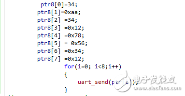
经过试验,从表象看,是串口影响了SDRAM的读取和写入。