Improving efficiency
Thank you.

Its efficiency may suffer from shoot -through current when the Mosfets switch.
It needs non-overlaping separate drive signals for the top and bottom Mosfets.
will it improve the efficiency? and can you tell me what components should I add to do so?
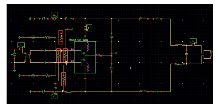
Is the "Power_Amp_Core" component, a Class D amplifier?
More details about this circuit would help.
It is a class c amplifier
I have found it most helpful to concentrate on the "elements
of inefficiency". Efficiency of the assembly is your report card.
Inefficiencies are what you quantify and drive down one by
one, as your homework.
Losses exist everywhere. You need to characterize the point
losses and assign their causes, in order to efficiently chase
inefficiency out and improve the bottom line.
But you never improve the bottom line by looking at the
bottom line.
In my DC-DC developments we had a smart kid who took
every "moving part" and figured its losses in Excel, using
the knowable attributes. This helped us optimize both
product and eval board to get the best showing.
You might find out that (for example) you lose more energy
per cycle in the input filter than the power switch. Yet
many would fixate on the active power path and ignore the
"ideal" (which there are none) components that "just sit
there".
Be sure you give the wallflowers their chance to dance.
Only if that is the cause of a large part of the inefficiency.
You need to analyze the circuit as dick suggested to determine where the inefficiency is coming from.
What is the present circuit efficiency?
Your inductor and capacitor values are not displayed. When you consider what values to choose:
* Inductors: Start with a small Henry value, and increase until it begins to restrict (or choke) current.
* Capacitors: Start with a large value, reduce until it begins to restrict current. When it's positioned so it acquires a DC charge, you usually get optimum performance if its charge doesn't drop too much during a cycle, say more than 5 or 10 percent.
Moved the thread to the RF section where it belongs.
You have positive Vgs bias which is probably inappropriate for class C, depending on the transistor threshold voltage and drice level. How did you design the bias voltage?
The load is cut from the schematic. Is the circuit designed with proper impedance matching? Did you check the matching, e.g. by load pulling method?
We also don't know if the power transistor is suited for the intended purpose. Did you design the circuit according to manufacturer suggestions?
Are you reporting hardware measurements or simulation results? What are the efficiency numbers?
