HFSS port 'Port1' does not have a valid reference plane above or below it.

I have managed to solved all the simulation issues, and make the simulation converged, but the s-parameter magnitude and phase results make the layout looks like not a marchand balun. Why ?
Note that the via is not visible at the end of each strip for ports 2 and 3. I am still trying to make the via visible
planar marchand balun

magnitude plot

phase plot

Did you forget the vias to short the end of the line?
@volker
No, I have put the via in place, but it is just not visible. How do I make the via visible in the layout widow display ?
I have now added the via correctly and the two vias are visible now.
However, the magnitude and plot simulation results remain unchanged. Why ?

I am not an HFSS user, but your vias look like circles on the metal layers, not like a vertical connection between the layers. Check what impedance into that line segment you see at DC.
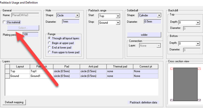
See the via parameter dialog setting

As I wrote: I am not an HFSS user, but I don't see that vertical metal connection. Not in your 3D view and not in your dialog. You just have the circles on the two metal layers. No connection in between.
I am just trying to replicate New Design Formulas for Impedance-Transforming 3-dB Marchand Baluns
Note: I have attached the entire project file (I am using Ansys Electronics Suite 2018.2) here


Did I mention that I am not an HFSS user? But this looks wrong to me. For EM simulation, a via requires a conductor.
Let me repeat: you can check the via if you check input impedance into path at DC. That works in real life - and in simulation as well.
I need to figure out a way to do this via impedance checking in HFSS.
Anyone else had experience checking via connectivity in HFSS ?
I have changed the material for both via to use FR4 epoxy, but the s-parameter magnitude and phase plots are still in a mess.

No no no ... wrong!
I think your misunderstanding is here:
- If you send PCB data to a manufacturer, you draw a drill hole and during processing, their metal plating will create the via contact.
- But here you are in EM simulation, no plating of drills is done behind the screnes, and you explicitely need to define a via layer with conductor material to create that connection.
In all EM simulations tools that I know, we create separate VIA layer with METAL, to make that connection between layers. From your dialog, maybe HFSS creates that via for you, but material must be METAL. Epoxy is wrong!
Checking the connectivity is easy, just look at S-parameters at DC, as mentioned before. S11 phase will tell you if there's an open or short.
I have changed the via material to copper , but the waveform results still do not look good at all.
The following are the S22 and S33 waveforms.

Show a plot of S22 phase and S33 phase, so that we can check if the via is there.
And maybe reduce your model to a simple 50 Ohm tru line, so that you can practice settings of materials and layers. I'm not even sure if you have the backside metalization in place, drawn as a conductor or realized as a PEC boundary condition.
backside metalization ? This is a 2 layer PCB.

See the S22 and S33 phase plots

Sure, 2 layers, and for such microstrip design the bottom layer is a solid ground plane. That's what I meant with backside metalization.
~~~
Your S22 and S33 shows 180° at DC, which is what we expect for a short circuit. So it looks like your vias are ok.
~~~
The gap (spacing) between coupled lines is much smaller in the photo that you showed. In your model, the spacing is much larger, on the order of the substrate thickness.
Another note: Your line at port 3 is very close to an edge. From your screenshots I can't see if that is the substrate edge, or ground plane edge, or both. I would add some extra margin there (rule of thumb: at least 2 * line width) , so that line impedance works as designed.
So, there is no issue with the stackup layer as well as the via settings ?
And why would phase of reflection coefficient gives 180 degrees for a short circuit ? I forgot the math.
I will fix the gap spacing between coupled lines as ell as the extra margin for port 3 and see if those solution help.
Something else is wrong. The gap sizing between coupled lines is smaller now, but then the s-parameter waveforms still unchanged.

Reduce the model to a simple thru line and check results. Most likely your feedline are 50 Ohm, so that test should be fairly easy.
Are you sure you have the correct dimensions for 20mil substrate thickness? I checked the dimensions from your table in #8 and it gives other Zoe/Zoo for these dimension, so it seems the substrate height in the paper was different.

wait, where did you get the information to use 4.3 for Er and 1.0 for Mur ?
μr=1 is physics, εr=4.3 is typical FR4 (but not as clearly defined as for good RF substrates, actual value might be as low as 3.9 or as high as 4.7 depending on resin/fibre mixture)
- Exporting HFSS design model to GDSII file.
- How to check recevied power in the HFSS port?
- Importing data from HFSS and ploting in matlab
- Defining Lumped port in 3D spiral coil for different values of sweep in HFSS
- HSS Port refinement Error
- Adding/Importing PCB enclosure(step/iges file) to HFSS 3D layout