crystal oscillator 起振后的怪现象
在hspice里面仿真时,可以起振,但起振后,放大器输出与晶振连接的地方振荡的中心电平会逐渐变低,导致后面的反向器无法翻转.设计要求负载电容用moscap在片内实现.用理想电容时,不会有这种现象.请问如何解决这个问题.
谢谢!
沒有附圖難以瞭解Crystal是RLC model?
是用什麼樣的放大器?
放大器的工作點是在1/2VC
Gain, Driving current...enough?
首先谢谢楼上的答复.由于我们内网和外网是分开的,自己不能抓图.只能描述一下了.
Crystal是用RLC model的.放大器是两个管子做成的反相器.
工作点是在1/2 vdd
工作电流和增益应该足够了.因为可以起振.只是起振后反相器输出的电平会下降.
电路结构如下图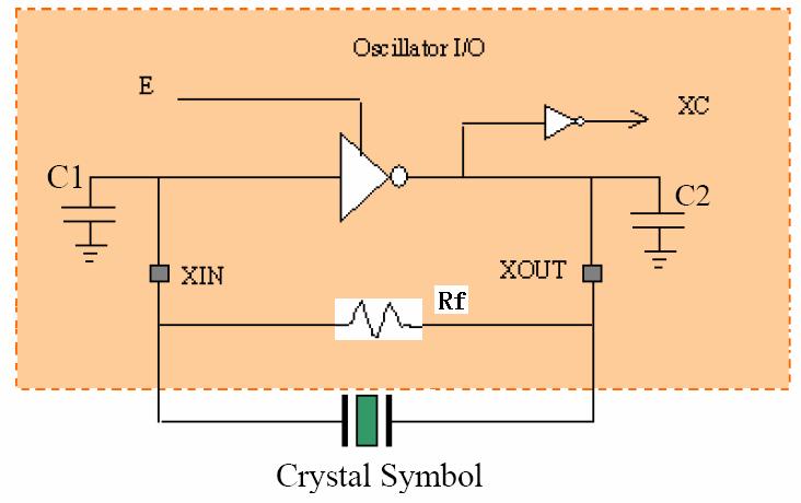
其中,Rf由传输门构成,C1和C2由moscap形成,晶体由RLC来建模.
CRYSTAL 是多少兆的
1. Check amplitude of V(C1) and V(C2). Is rail to rail?
2. Check CM of V(C1) and CM of V(C2), Is that equal?
3. Check amplitude of V(C2)see if stable( means no more increasing already)
4. Normally, current will be up and down, up and down and stable in average.
5. If properly design, MOSCAP and Ideal CAP does not have that much difference in current but they doimpact the stability of oscillation frequency since CV of MOSCAP.
谢谢各位的答复.
crystal是12M的.
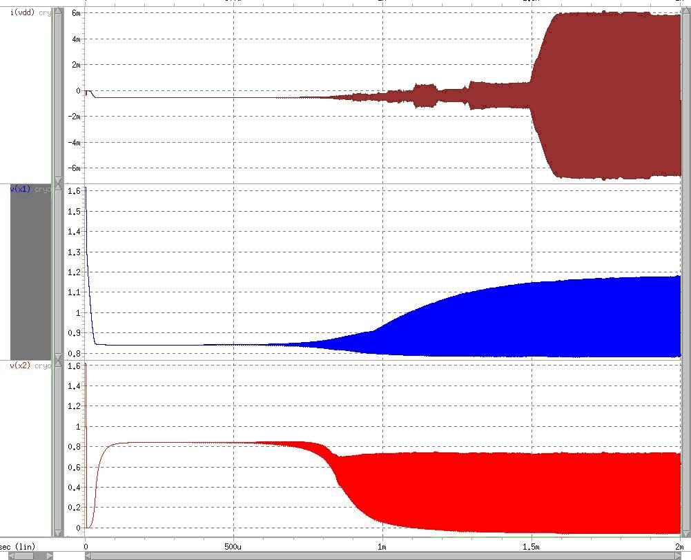
vc1 and vc2 are not rail to rail (in hspice), and are both rail to rail and even larger than rail to rail (in spectre)
CM of vc1 and vc2 are first equal, but suddenly one increase and the other decrease.
here are some pictures, but they are not all, I will provide the other later.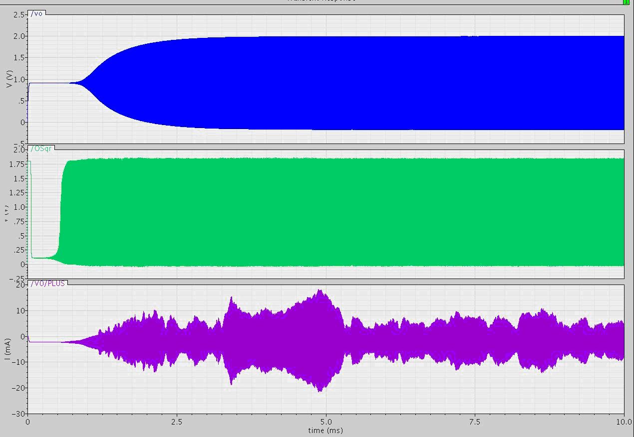
the top curve is the vc2, the middle curve is the output after buffers, the bottom curve is the total current in spectre

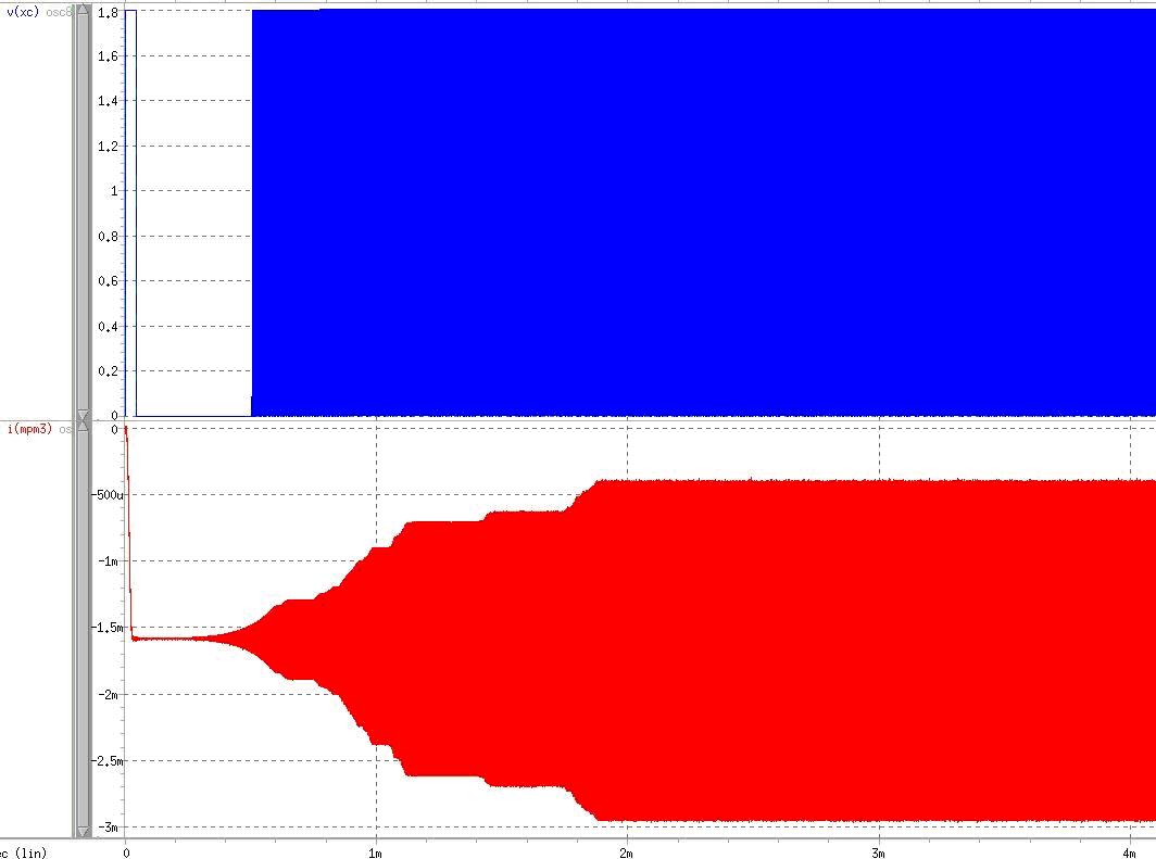
the top curve is the output after buffer, the bottom curve is the total current, and the transient current has been more than 100mA (in spectre)
the top curve is the output after buffers, the bottom curve is the total current in hspice
Thank you very much!
simulation results in hspice
tt
SS
thank you very much!
这应该是个pierce 振荡电路吧
1. What is the size of the two inverter?
2. Enlarge the waveforms after 7.5ms (this is ridiculous big in current) and see what the waveform looks like
进来学习,我的project也要用到同样的Pierce Crystal Oscillator
Thank you for all your replies.
The size of the inverter is NMOS: 4*48/0.7 PMOS: 4*9/0.7. I know the ratio of their size is a little strange, but otherwise I couldn't get a VCM near the Vdd/2.
Some of my colleagues thought that the reason may come from the discontinuity of the model.
hi
NMOS --- 48/0.7, M=4;
PMOS --- 9/0.7, M=4;
Maybe you should decrease the size of NMOS & increase the PMOS size.
For example, let NMOS size : 4*12/0.7, & PMOS : 4*24/0.7
you can try.
Thanks.
I will have a try.
应该是PMOS的宽长比大些的
"
hiNMOS --- 48/0.7, M=4;
% k. K6 t4 T- ?" E0 NPMOS --- 9/0.7, M=4;
+ N* w" y% w/ ~% [" l0 x" [I& M3 B0 k' i6 _) J$ a
Maybe you should decrease the size of NMOS & increase the PMOS size.' Z9 O9 k/ [) Z# Z5 W
For example, let NMOS size : 4*12/0.7, & PMOS : 4*24/0.7 : K7 h) o9 ~8 o% p/ T
- K- d/ n# x% L% j' {, R! F/ k
you can try.
"
Thank you.
To tell the truth, your crystal ciruit design is still at very low level because
(1) Inverter based XTAL circuit is very power consuming and distorted.
(2) Inverter based XTAL circuit has very bad frequency stability of oscillation and therfore high jitter
(3) Inverter based XTAL circuit also impacts on XTAL life( too high DL)
only advantage is --- simple
May I suggest
(1) Still keep pierce type, but change to class A amplifier
(2) I understand you wanna keep VCM at VDD/2, this is good. Few people has this idea. You can do it using another DC loop to make it instead of using abnormal PMOS/NMOS ratio, just as you did now.
(3) If you wanna more complicate, I also sugget you add amplitude control.
If you did all of three, you are now at least entering advanced level.
Of course, you don't care about the performance. Pls, just keep inverter!
Thank you very much.
All suggestions are very good points. I'll try them.
BTW, what's DL?
Thanks!
好像是MOSCAP有寄生的电阻,影响了反馈回路
我也觉得inverter的设置出现问题了, 你首先做了ac仿真吧,查看下起振的充分条件是否满足
3ks
22# hi_china59
Thank you.
多久的老帖子还被翻出来了
输入输出工作点出现反方向变化的原因是什么?
我的理解是输出端信号出现强非线性,其平均值跟输入点的直流值之间有差,需要通过
原理图里对低频信号的负反馈回路来以抑制工作点的变化,而仿真如果表现出来这个反馈不起作用,说明反馈失效了,可能的原因只能是那个连接到输入端的MOSCAP有等效电阻到地,且值与Rf可比拟或者还要小,这就导致低频信号不能100%跟随。
假设输出出现100mv偏差,本来需要-1的反馈系数来达到跟随的目的,现在因为这个寄生电阻的存在导致反馈量不够,输出就不能回到工作点,如果输出的非线性加剧,可能最后会导致电路工作点彻底不正常。
我靠,很好的一帖,一定认真学习一下!
22# hi_china59
我的Crystal oscillator也不能起振
Cool diacussion,
学习了