使用STM32 Timer的Gate模式来精确控制脉冲个数
用到了Timer Master Slave中的Gate模式
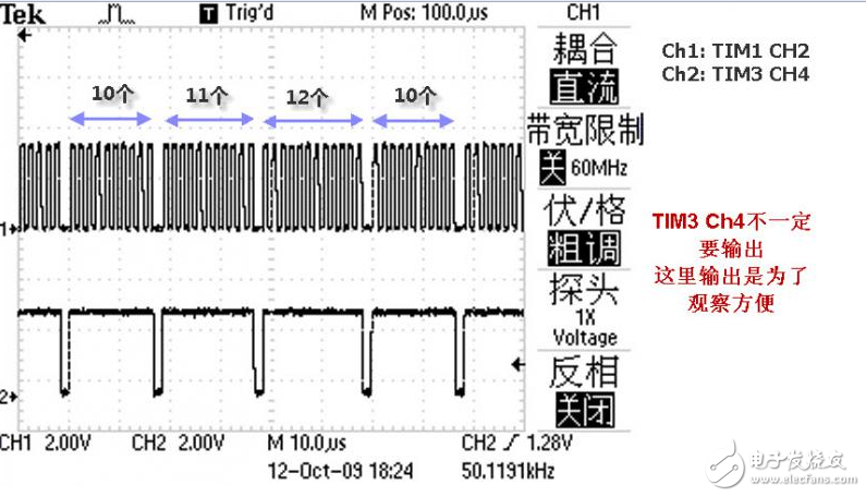
比如TIM1输出PWM, 频率为F
可以用TIM2通过Gate来控制TIM1的输出
将TIM2预频设为1/(F*2),则TIM2的Period 就是 脉冲个数*2 - 1
/* 1 2 3 4 5 6 7 8 9
__ __ __ __ __ __ __ __ __
| | | | | | | | | | | | | | | | | |
TIM1: ___| |__| |__| |__| |__| |__| |__| |__| |__| |____________________
->| Period1|<-
1) 2) 3) 4) 5) 6) 7) 8) 9) 10)11)12)13)14)15)16)17)
__________________________________________________
| |
TIM2: ___| |____________________
->| |<--- Pres2 = Period1/2
|<------------ Period2 = N*2-1 = 17 ------------>|
*/
实现代码
软件:
IAR 4.42限制版
ST库 2.01
硬件:
万利199开发板 STM3210B-LK1
/*0001*/ /* Includes ------------------------------------------------------------------*/
/*0002*/ #include "stm32f10x_lib.h"
/*0003*/
/*0004*/ /* Private typedef -----------------------------------------------------------*/
/*0005*/ /* Private define ------------------------------------------------------------*/
/*0006*/ /* Private macro -------------------------------------------------------------*/
/*0007*/ /* Private variables ---------------------------------------------------------*/
/*0008*/ ErrorStatus HSEStartUpStatus;
/*0009*/
/*0010*/ /* Private function prototypes -----------------------------------------------*/
/*0011*/ void RCC_Configuration(void);
/*0012*/ void NVIC_Configuration(void);
/*0013*/ /* Private functions ---------------------------------------------------------*/
/*0014*/
/*0015*/ #define PWM_Period 120
/*0016*/ int main(void)
/*0017*/ {
/*0018*/ u16 waveNumber = 10;
/*0019*/ /* System Clocks Configuration */
/*0020*/ RCC_Configuration();
/*0021*/
/*0022*/ /* Enable related peripheral clocks */
/*0023*/ RCC_APB2PeriphClockCmd( RCC_APB2Periph_GPIOA,ENABLE);
/*0024*/ RCC_APB2PeriphClockCmd( RCC_APB2Periph_GPIOB,ENABLE);
/*0025*/ RCC_APB2PeriphClockCmd( RCC_APB2Periph_TIM1,ENABLE);
/*0026*/ RCC_APB1PeriphClockCmd( RCC_APB1Periph_TIM3,ENABLE);
/*0027*/
/*0028*/ /* Config IO for related timers */
/*0029*/ {
/*0030*/ GPIO_InitTypeDef GPIO_InitStructure;
/*0031*/ /* Timer1 Channel 2, PA9 */
/*0032*/ GPIO_InitStructure.GPIO_Pin = GPIO_Pin_9;
/*0033*/ GPIO_InitStructure.GPIO_Mode = GPIO_Mode_AF_PP;
/*0034*/ GPIO_InitStructure.GPIO_Speed = GPIO_Speed_50MHz;
/*0035*/ GPIO_Init(GPIOA, &GPIO_InitStructure);
/*0036*/ /* Timer3 Channel 4, PB1*/
/*0037*/ GPIO_InitStructure.GPIO_Pin = GPIO_Pin_1;
/*0038*/ GPIO_Init(GPIOB, &GPIO_InitStructure);
/*0039*/ }
/*0040*/ /* Setup Timer3 channel 4, Timer3 is master timer
|*0041*| This timer is used to control the waveform count of timer1 */
/*0042*/ {
/*0043*/ TIM_TimeBaseInitTypeDef TIM_TimeBaseStructure;
/*0044*/ TIM_OCInitTypeDef TIM_OCInitStructure;
/*0045*/ TIM_DeInit(TIM3);
/*0046*/ TIM_TimeBaseStructInit(&TIM_TimeBaseStructure);
/*0047*/ TIM_OCStructInit(&TIM_OCInitStructure);
/*0048*/ TIM_TimeBaseStructure.TIM_Prescaler = PWM_Period/2 - 1;
/*0049*/ TIM_TimeBaseStructure.TIM_CounterMode = TIM_CounterMode_Up;
/*0050*/ TIM_TimeBaseStructure.TIM_Period = waveNumber*2;
/*0051*/ TIM_TimeBaseStructure.TIM_ClockDivision = TIM_CKD_div1;
/*0052*/ TIM_TimeBaseInit(TIM3,&TIM_TimeBaseStructure);
/*0053*/
/*0054*/ /* Timer2 Channel 3 Configuration in PWM2 mode, this is used for enable Recive clcok */
/*0055*/ TIM_OCInitStructure.TIM_OCMode = TIM_OCMode_PWM1;
/*0056*/ TIM_OCInitStructure.TIM_OutputState = TIM_OutputState_Enable;
/*0057*/ TIM_OCInitStructure.TIM_Pulse = waveNumber*2 - 1;
/*0058*/ TIM_OCInitStructure.TIM_OCPolarity = TIM_OCPolarity_High;
/*0059*/ TIM_OC4Init(TIM3,&TIM_OCInitStructure);
/*0060*/ TIM_CtrlPWMOutputs(TIM3, ENABLE);
/*0061*/ TIM_SelectOnePulseMode(TIM3, TIM_OPMode_Single);
/*0062*/ }
/*0063*/ /* Setup timer1 channel 2, Timer1 is slave timer
|*0064*| This timer is used to output waveforms */
/*0065*/ {
/*0066*/ TIM_TimeBaseInitTypeDef TIM_TimeBaseStructure;
/*0067*/ TIM_OCInitTypeDef TIM_OCInitStructure;
/*0068*/ TIM_DeInit(TIM1);
/*0069*/ TIM_TimeBaseStructInit(&TIM_TimeBaseStructure);
/*0070*/ TIM_OCStructInit(&TIM_OCInitStructure);
/*0071*/ TIM_TimeBaseStructure.TIM_Prescaler = 0;
/*0072*/ TIM_TimeBaseStructure.TIM_CounterMode = TIM_CounterMode_Up;
/*0073*/ TIM_TimeBaseStructure.TIM_Period = PWM_Period;
/*0074*/ TIM_TimeBaseStructure.TIM_ClockDivision = TIM_CKD_div1;
/*0075*/ TIM_TimeBaseInit(TIM1,&TIM_TimeBaseStructure);
/*0076*/
/*0077*/ /* Timer2 Channel 3 Configuration in PWM2 mode, this is used for enable Recive clcok */
/*0078*/ TIM_OCInitStructure.TIM_OCMode = TIM_OCMode_PWM1;
/*0079*/ TIM_OCInitStructure.TIM_OutputState = TIM_OutputState_Enable;
/*0080*/ TIM_OCInitStructure.TIM_Pulse = PWM_Period/2;
/*0081*/ TIM_OCInitStructure.TIM_OCPolarity = TIM_OCPolarity_High;
/*0082*/ TIM_OC2Init(TIM1,&TIM_OCInitStructure);
/*0083*/ TIM_CtrlPWMOutputs(TIM1, ENABLE);
/*0084*/ }
/*0085*/ /* Create relationship between timer1 and timer3, timer3 is master, timer1 is slave
|*0086*| timer1 is work under gate control mode, and controled by timer3
|*0087*| timer3's channel 4 is used as the control signal
|*0088*| */
/*0089*/ /* Enable timer's master/slave work mode */
/*0090*/ TIM_SelectMasterSlaveMode(TIM3,TIM_MasterSlaveMode_Enable);
/*0091*/ TIM_SelectMasterSlaveMode(TIM1,TIM_MasterSlaveMode_Enable);
/*0092*/ /* timer3's channel 4 is used as the control signal */
/*0093*/ TIM_SelectOutputTrigger(TIM3,TIM_TRGOSource_OC4Ref );
/*0094*/ /* Check the master/slave is valid or not */
/*0095*/ compile_assert((u16)GetInternalTrigger(TIM1,TIM3) != (u16)-1);
/*0096*/ /* Config timer1's external clock */
/*0097*/ TIM_ITRxExternalClockConfig(TIM1, GetInternalTrigger(TIM1,TIM3));
/*0098*/ TIM_SelectSlaveMode(TIM1,TIM_SlaveMode_Gated);
/*0099*/
/*0100*/ /* Enable the slave tiemr*/
/*0101*/ TIM_Cmd(TIM1,ENABLE);
/*0102*/ //SetupAlltimers();
/*0103*/ while(1){
/*0104*/ /* Check whether the previous action is done or not */
/*0105*/ if(!(TIM3->CR1 & 1)){
/*0106*/ TIM1->CNT = 0; /* It would be very perfect if gate mode can
|*0107*| reset the slave timer automatically */
/*0108*/ TIM3->ARR = waveNumber*2; /* Reload wave number*/
/*0109*/ TIM3->CCR4 = waveNumber*2 - 1;
/*0110*/ TIM3->CR1|=1; /* Re-enable the timer */
/*0111*/ /* update waveform number */
/*0112*/ waveNumber++;
/*0113*/ if(waveNumber == 13){
/*0114*/ waveNumber = 10;
/*0115*/ }
/*0116*/ }
/*0117*/ }
/*0118*/ }
/*0119*/
/*0120*/ /*******************************************************************************
|*0121*| * Function Name : RCC_Configuration
|*0122*| * Description : Configures the different system clocks.
|*0123*| * Input : None
|*0124*| * Output : None
|*0125*| * Return : None
|*0126*| *******************************************************************************/
/*0127*/ void RCC_Configuration(void)
/*0128*/ {
/*0129*/ /* RCC system reset(for debug purpose) */
/*0130*/ RCC_DeInit();
/*0131*/
/*0132*/ /* Enable HSE */
/*0133*/ RCC_HSEConfig(RCC_HSE_ON);
/*0134*/
/*0135*/ /* Wait till HSE is ready */
/*0136*/ HSEStartUpStatus = RCC_WaitForHSEStartUp();
/*0137*/
/*0138*/ if(HSEStartUpStatus == SUCCESS)
/*0139*/ {
/*0140*/ /* Enable Prefetch Buffer */
/*0141*/ FLASH_PrefetchBufferCmd(FLASH_PrefetchBuffer_Enable);
/*0142*/
/*0143*/ /* Flash 2 wait state */
/*0144*/ FLASH_SetLatency(FLASH_Latency_2);
/*0145*/
/*0146*/ /* HCLK = SYSCLK */
/*0147*/ RCC_HCLKConfig(RCC_SYSCLK_Div1);
/*0148*/
/*0149*/ /* PCLK2 = HCLK */
/*0150*/ RCC_PCLK2Config(RCC_HCLK_Div1);
/*0151*/
/*0152*/ /* PCLK1 = HCLK/2 */
/*0153*/ RCC_PCLK1Config(RCC_HCLK_Div2);
/*0154*/
/*0155*/ /* PLLCLK = 8MHz * 9 = 72 MHz */
/*0156*/ RCC_PLLConfig(RCC_PLLSource_HSE_Div1, RCC_PLLMul_9);
/*0157*/
/*0158*/ /* Enable PLL */
/*0159*/ RCC_PLLCmd(ENABLE);
/*0160*/
/*0161*/ /* Wait till PLL is ready */
/*0162*/ while(RCC_GetFlagStatus(RCC_FLAG_PLLRDY) == RESET)
/*0163*/ {
/*0164*/ }
/*0165*/
/*0166*/ /* Select PLL as system clock source */
/*0167*/ RCC_SYSCLKConfig(RCC_SYSCLKSource_PLLCLK);
/*0168*/
/*0169*/ /* Wait till PLL is used as system clock source */
/*0170*/ while(RCC_GetSYSCLKSource() != 0x08)
/*0171*/ {
/*0172*/ }
/*0173*/ }
/*0174*/ }
效果如下图
转自bbs.ednchina.com/BLOG_ARTICLE_2001185.HTM