关于电压偏置设计的问题,芯片外v.s. 芯片内
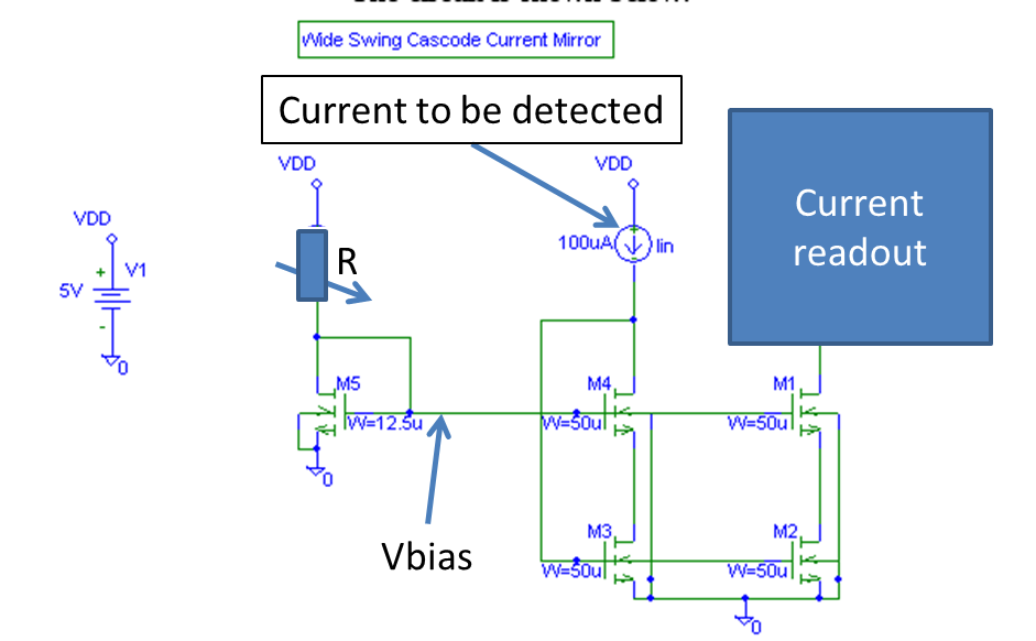
大家好,下图中的wide swing current mirror 的偏置由M5和可变电阻R共同产生,可变电阻R在片外。把这种方法称为方法1。
在方法2中, 把M5和R去掉,通过仿真确定M1和M5偏置电压,直接由片外可变电压偏置(电阻分压桥+buffer)提供这个偏置电压,哪个方法好些?
请注意,Iin是待检测电流,是可变的。另外,我是个学生,是在设计一个prototype而不是产品。
图片看不到!
no Tu 图!
原来是直接粘贴,现在已插入图片。
都很小吧,最大的噪声源来自Iin或者M2、M3
I strongly recommend you to use method 1.Considering technology variation, you cannot control the bias well through direct voltage biasing.
and remember never use method 2, no one use it.Method 1 is always better. We only consider using current mirror to bias integrated circuits.
Even you can generate voltage through bandgap reference, finally use current mirror to bias some circuits, never use the output voltage of bandgap reference directly. Otherwise, strange things happen and you don't know why.
多谢回答!
多谢指点。我想我没有说清楚,已经更新了原帖。这里我再说下,这里Iin是待检测电流,是可变的,M1和M4的偏置电压需要一个固定值。我在考虑原帖中的两种方法去产生这个偏置,在方法1中,Ibias是片外,在方法2,电压偏置直接从片外提供。
小编什么画图软件
This is what I mean. Method 1 is always better whatever you design.
好吧,这句是重点,多谢小编解疑!
我直接从论坛粘过来的。不过我认为是LTSPice之类的仿真软件吧。
好象 很经典 方法1............
seeing