求助一个可调延迟的反相器电路
时间:10-02
整理:3721RD
点击:
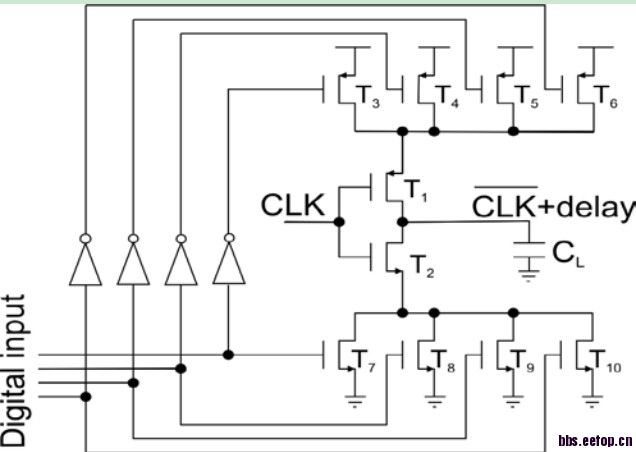
今天看论文看到一篇讲到了上述的这个电路...以及它对应的仿真曲线...从电路图上直观的看..数字信号开启的PMOS和NMOS管越多,对应充放电电流越强,应该延迟越短..可是为什么论文中给出的结论却正好是相反的呢...?
自己顶起...希望大家能帮帮忙..
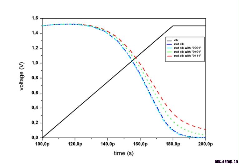
蓝色的那根not clock 是什么设定
这个论文中没有提到,关于这个结果的描述如下:a combination of transistors are turned on. By variation of
the digital input bits, the delay can be increased and decreased.
Fig.5shows the delay for different input bit vectors. For
reasons of clarity not all bit combinations are shown. The
other delays lie between the presented lines. This concept
ensures a controlled delay of the rising and falling edge that
corresponds to a time delay of the whole signal, as needed for
the trimming of the comparator.
我认为这个蓝色的可能表示未进行调节时的曲线(就是没有上面的一排PMOS和下面的一排NMOS)
我也感觉反的--!
看不出有什么玄机
再顶起...求助...我仿出来的结果也和这个不一样...不知道是因为管子大小取值的问题..还是说这个文章的问题..
这是我仿的结果

我仿出来也是开启的管子越多,上升/下降时间越快...看来是文章弄错了可能
需要点怀疑精神啊
可以share一下这篇paper吗