我的锁相环的控制电压VC跳动很大,高手进来看看是为什么?

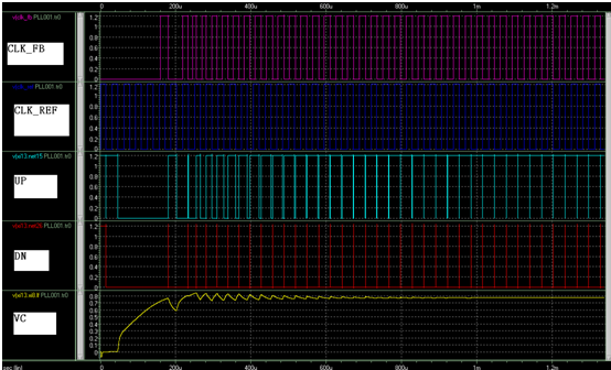
输出1MHZ仿真图

输出1MHZ局部放大图(控制电压VC上有150mV的跳动)

PLL相关参数
我的锁相环采用的是普通的电荷泵结构,补偿网络采用两个电容和一个电阻的二阶补偿,仿真结果看控制电压VC跳动很大,导致输出结果不对。不知道是什么原因?我的环路相位裕度是50度,怎么看起来仿真结果像是不稳定!大家来看看是什么原因,谢谢!
主要是CP的mismatch比较大的缘故。

CP线路图
2M输出时仿真波形

2M输出时局部放大图

2M输出时PLL参数
谢谢关注!CP线路如上图所示,只是采用最普通的P,N,MOS管充放电,当相位差为0时,充放电管关闭,VC悬空。
输出为2MHZ时,仿真结果却是正常,控制电压VC上有5mV的跳动,同样的线路。
只是反馈分频系数和滤波网络的R2值不同。疑惑啊!
可能是带宽太大了。
pll还有一个带宽最好小于比较器频率1/10的稳定性要求,你可以尝试改变一下输入频率,但不改变系统带宽仿真看看是不是违反了这个要求。
你看输出1MHZ局部放大图中第一个信号,应该是vco分频后进入pfd的时钟吧,这个相位和频率变化太快了,应该不是vco随压控电压变化的现象,所以我怀疑你的分频器可能有问题,不能工作在分频成1M的分频比上。

我数了一下分频结果,分频器是正确的,CLK_FB变化大是VC跳变大,导致VCO输出时钟变化大导致的
很有可能,我把CLK_REF改成64KHZ试试。
输出是500KHZ的VC跳变小一些,大概40mV。
输出500KHZ时的仿真图

输出500KHZ局部放大图(控制电压VC上有40mV的跳动); TCLKOUT=2.1uS~2.61uS

输出500KHZ时PLL的参数
谨慎怀疑你的CP有问题
你有没有在CP中加buffer让P跟N电流源永远处于导通状态
而不是一直在on off
CP线路在3楼有,你帮忙看一下,有没有问题,没怎么看明白你的意思,你的意思是我有没有设置电荷泵处于同时充放电的状态?望详解。
我的意思是:
在一个时间点P或者N管其中一个连接到capacitor,冲/放电
这时另外一个处于关闭状态
但这样不是很好,
因为你需要不停的开关电流源,
瞬态电流很难准确控制
利用voltage buffer可以使两个电流源一直处于打开状态,
只利用开关改变电流流通方向
这样电流源的电流大小更加稳定
同时VC也更加稳定
这个CP结构是自己设计的吗?好像不多见这么用的,楼上的问题的确值得参考,而且用电流源加开关结构可能会比现有结构好些。另外,电流源同时开的问题可以在PFD设计中解决。
减小环路带宽后输出为1MHZ时的仿真结果
局部放大1

局部放大2

局部放大3(前一个图的下个周期)

调节了补偿电阻R2,改变了减小了环路的带宽,输出控制电压VC跳动明显减小,最后为1mV左右,但是最终还是达不到上下管子同时导通的状态,前一个周期在DN脉宽为最小脉宽0.5ns,UP脉宽逐渐缩小为40ns后,下一个周期直接跳到UP为最小脉宽0.5nS,DN脉宽为20nS,这两个周期后面在来回切换,就是达不到上下管子同时导通为0.5ns的状态)。不知道是什么原因?
关注。
想起来半年前有人说他的pll spur为什么在1/2fref频率上出现,现在看你这个,岂不是也在1/2fref频率上有spur?当时那个讨论http://bbs.eetop.cn/viewthread.p ... p;extra=&page=2没有下文了,我给的linkedin上那个讨论倒是给出了不少假设,既然是仿真,你可以根据他们的假设逐一验证一下哪个符合你的情况。
环路带宽至少应该是 参考频率的1/4, 否则会有 sampling effect 出现,你的第一个图片应该是出现了sampling effect
线路是在以前流片过的线路基础上修改的,并且换了工艺。
好的,那个网站进不去要先注册,我刚注册了,在等批准
说的有道理,改了带宽以后,VC跳动减小到几mv了,但是最后就是不会上下都到最小脉冲状态,有可能就是CP的问题
你说的网站我加不进去了,能否将讨论的内容复制到这里,万分感谢!
讨论很长,copy格式有些乱。What mechanism can create fref/2 spurious in a fixed integer divider pll ?
10 months ago
- Like
- Comment
- Follow
- Flag
- More
Yanjie Sun likes this
62 comments • Jump to most recent comments
Follow André
André Fivaz • Maybe one thing to consider: A change in impedance at the divider input (frequency pulling between high/low states), it may be necessary to isolate the VCO by an extra amplifying stage
9 months ago• Like
Follow Jean-Francois
Jean-Francois Debroux • Thanks André for your suggestion. I'll consider it. Anyway, some memory effect is definitely to exist somewhere to generate fref/2...
9 months ago• Like
Follow Qiang
Qiang Lin • In my experience, most likely it is generated in the circuit somewhere then coupled to VCO. It could be in the divider or some other circuits indirectly related to the PLL, thus easily overlooked.
9 months ago• Like
Follow Lawrence
Lawrence Ragan • Is the reference clock used anywhere else? If there is divider hanging on it somewhere, you could be getting fref/2 signals on the supply or ground rails.
9 months ago• Like
Follow Hedley
Hedley Rokos • Is this something that you see on the physical circuit but not in simulations?
Does the PFD have different gain at the decision point than the design value?
Such effects would be quite variable..
Otherwise:
a) Are you able to check the spectral content of Fref itself?
b) You can in principle get pumped resonance problems also if the loop gain is large - but this should show up (at least as a noise peak) in simulations.
c) Simulations should also be able to show if the power supplies are pulled down by alternate cycles of the phase-frequency comparator.
d) Ditto power supply resonances
(I'm trying to avoid repeating other good suggestions)
• Like
IconomosUnfollow
Iconomos Koullias • You may be having instability (oscillation) during the transition periods due to insufficient signal level drive, too fast (or too slow) circuit, etc. Under those conditions, dividers many times act like mixers with feedback from output to one of the inputs that cause them to oscillate at half the input frequency. I have seen it in ICs more than once. Increasing the input signal level, decreasing the feedback capacitance, increasing or decreasing the circuits frequency response (oscillation response has an optimum frequency), lower ground/supply inductance, better pin-out usually takes care of the problem. Good luck, I hope it helps.
9 months ago• Like
Follow Jean-Francois
Jean-Francois Debroux • Thanks to all for your ideas. I am currently looking at the PFD that seems to have an effect. It seems that it is a dead zone issue that disappears when the delay to reset is increased but I still don't know how this creates fref/2.
9 months ago• Like
Follow George
George Storm • PFD designs that exhibit dead bands will always generate spurious outputs unless appropriate action is taken, The spurious output can be noise or it can be a pure frequency. Its form and level will depend on the width of the dead band, the response of the loop, the level of the offsets in the loop, and the noise that is present. Adjusting relative timings so that the dead band becomes narrow can reduce the effect, but tolerances mean that this will never remove it entirely.
You can move the equilibrium point away from the dead band in a number of ways. The simplest is to provide a deliberate DC offset current at the output to the PFD; however, this will cause output to be generated at Fref itself unless the system also includes a suitably timed sample and hold circuit. An alternative method might be to inject a pulse of the same magnitude as the PFD pulses, and that is timed so the PFD output will cancel it. You can also use a collection of PFDs that have different timings, so that the total PFD gain never falls below some defined fraction of the nominal value; but this requires a lot of attention to detail if Fref injection is to be avoided. .
• Like
Follow Chuan
Chuan Wang • I've once met the same problem before. Iconomos Koullias's suggestion is really helpful. According to our debug, the divider, concoincide with the coupling effec (from the output to input, even to the VCO core), results of this issue.
9 months ago• Like
Follow George
George Storm • @ Iconomos Koullias
Am I misinterpreting what you write? As I read it your analysis includes that the loop divider gives an incorrect division ratio (a problem that is known with slow inputs + crosstalk in many designs of divider). However, this would result in an (easily identified) incorrect output frequency.
Or are you suggesting that the final stage of the divider (which correctly gives Fref as its output frequency) would give a different delay in alternate cycles of its output? Personally, I have only seen such effects when f/2 is explicitly present somewhere in the system (though this could happen if power supplies are inadequate).
@ Chuan Wang
You write after M. Debroux has observed that changing the delay of the reset in the PFD "cures" the problem. Are you proposing that the problem is an interaction between the PFD and the divider?
• Like
Follow Kin-wah
Kin-wah Kwan • One of the reason that might cause the phenomena is the charge pump.
The charge pump will be pumping and draining the LPF( capacitance ) at a frequency of fref/2. The LPF waveform, if enlarged, should show a rising and falling sawtooth waveform of fref/2. This effect should be small if the VCC/ground decoupling is good between charge PFD and VCO, and also the loop filter bandwidth is smalll enough.
• Like
Follow George
George Storm • @Kin-wah Kwan The question as I read it is "Why is there pumping at Fref/2?". You answer as if it was a universal property of charge-pump controlled loops, whereas it is in reality rather unusual.
You will usually get a modest component at Fref (due to asymmetries), with additional noise-like sidebands that correspond to the partial correction of the intrinsic movement of the controlled oscillator.
A component at Fref/2 corresponds to the charge-pump pumping in opposite directions in alternate cycles. The most common cause would be a combination of interaction between the dead band and a conditionally-stable loop, combined with the non-linear loop interaction locking the noise to the clock
• Like
Follow Jean-Francois
Jean-Francois Debroux • @Kin-wah, the staedy state VCO input voltage looks like a high pass filtered square signal at fref/2 (slope on the high and low levels). But apart what George states, I see no good reason for it to be at fref/2. It looks like it is an interaction between PFD dead zone and loop transient response. I am investigating the dead zone issue (that should not exist with this design) and will let the group know.
9 months ago• Like
Follow Kin-wah
Kin-wah Kwan • I only make a suggestion. It is up to you to take it.
Assume the loop in not locked precisely at the correct frequence. Then at the 1st reference clk, the PFD pull the VCO freq down. The next reference clk, the PFD will pull the VCO freq up. It is always a granular modulation going on- even for a stabel loop- just how large it is. And this modulation is at fref/2.
• Like
Follow Hedley
Hedley Rokos • Fref/2 oscillation can only happen with loops that are fast compared with the sampling frequency (clearly the loop gain at Fref/2 needs to be greater than unity).
. The oscillation amplitude will be unlimited if the loop is unstable at its nominal gain, so we have to conclude that M. Debroux's loop is conditionally stable. Note that it is always possible for conditionally stable loops to be triggered into oscillation if a deadband coincides with a loop equilibrium condition.
. If we assume a type II loop, this can be made be unconditionally stable if the integrator zero is sufficiently spaced below both the sampling frequency and any higher-frequency poles. This is the approach that I would take unless aquisition and/or tracking performance demand a more critical loop. Even for non-critical applications I would still prefer not to have a dead band unless I knew that phase wander slightly beyond the edges of the band was acceptable.
. True type III (and higher) loops cannot be unconditionally stable, and are therefore incompatible with designs where the equilibrium state of the control loop would set the PFD within the dead zone. [This note is for "completeness" only, as such loops typically show problems at lower frequencies.]
. In my experience* PFD designs that can have dead bands can be adjusted to limit the gain variation. However, the practical level of such gain variation would need to be assessed by extensive tolerancing, and the worst-case interaction with the loop assessed. One option would be to offset the loop so that equilibrium does not lie within the the dead band (as proposed elsewhere).
*admittedly limited, but there seem to be a-priori reasons to expect this constraint to be more general
• Like
Follow Hedley
Hedley Rokos • P.S. Perhaps we should also consider the possibility that the PFD has gain in its central band region that is greater than unity (the converse of a dead-band). My reasoning is that it takes quite a lot of effort to create a conditionally stable design with greater than unity gain at such a high frequency (half the sampling rate), and an increase in loop gain would readily cause an "unconditionally stable" loop to become oscillatory. The problem here is that this is not apparently compatible with M. Debroux's observation that "increasing the delay on the reset" improves matters; however, it may be that varying naming conventions are clouding the issue.
. We may be able to confirm the situation by modifying the loop gain (leaving all filter frequencies unchanged).
. If the loop remains stable (i.e. minimal change in sideband level) when the gain is doubled we can be confident that the problem is caused by a dead band. Oscillation under these conditions, however, is not proof that the cause is a high-gain region.
. To demonstrate that the cause is a high-gain region we need to exclude dead-band as a cause. For this we need to look at the effect of incrementally small decrements to the gain. An increased sideband level at some level of reduced gain demonstrates that the effect can be caused by a dead band. Fortunately (given the relatively high frequency of oscillation relative to the sampling frequency), any such effect should appear by the time the loop gain has reduced a factor of three. The downside of this method is that unstable gain range could be quite narrow...
. A simpler method would be to know the frequency-gain characteristics of the loop.
• Like
Follow Jean-Francois
Jean-Francois Debroux • Thanks Hedley. I notice that changing the filter (even though I don't have much flexibility in the design) does not change the picture. The nominal sizing is that the loop BW is about fref/10, changing it by an octave in any direction does not change anything. My latest investigations tend to show that PFD has a gain peak around 0 for a reason I will now try to find...
9 months ago• Like
Follow Jean-Francois
Jean-Francois Debroux • @Kin-wah, normally, the loop converges and does not create fref/2 even though I agree with the fact the operation is discrete. If the PFD generates short and identical UP and DOWN pulses, the spurious is at fref. Generating fref/2 requires something else. I am still investigating.
9 months ago• Like
Follow Kin-wah
Kin-wah Kwan • It is a general principle.
Traditioanlly, we use linease phase detector like multipiers that does not have deadzone, but linear phase error output at around 0-phase error. For these type of PLL, the granular stucture is definity fref/2. Not fref. You can use a mathematic tool for PLL to demonstration this effect!
For PFD,there is a dead zone where the phase comparator cannot give a phase error output when phase error is small. To linearize the region at this balance operation, designers usually add a slight offset to the output, in terms of charge pump leakage so that at equilibrim point, the PFD will pull the VCO away from the balance point, and the next comparation cycle will pull it back to the balance point again. This will give the observation of fref, as the the pull out and pull in all happen within a fref cycle.
These are all welknown facts and I am not going into discussion further.
For the low bandwidth of BW=fref/10 , it looks like you cannot get a good filtering / averaging for the phase error. I would not comment this further and let others have a chance to give their view.
• Like
Follow Hedley
Hedley Rokos • @Kin-wah
. I think I now understand your starting-point - a phase detetector that is an XOR gate or a mutiplier. The characteristics are of course quite different from the sort of PFD that Jean-Francois described.
. There is however still a major issue: my mathematics (supported by experience) does not find the injected sidebands ("granular structure") at Fref/2: indeed, the expected frequency for these is 2*Fref.
• Like
Follow Hedley
Hedley Rokos • Jean-Francois:
. "the loop BW is about fref/10"
. Thank you for the clarification. I too cannot see any way that a dead-band in such a loop could generate Fref/2 if everything else was "normal". Indeed, the effect you are seeing is way outside my experience.
So I become ever more tentative.
Nevertheless, I believe that one would need one of the following (or a combination of effects):
. Interaction via power supplies*
. (this could include supply impedance resonances or bistability)
. more-than 5x the PFD gain at the equilibrium pont,
. a PFD that is sensitive to disturbance while in its dead-band
. (and a source of such disturbance)
. an amplifier wihin the loop that has a resonance near Fref/2*,
. an non-analysed differentiator within the loop (unlikely?)
. crosstalk that mimicks high gain at Fref/2* (ditto?)
* Most of these would change their behaviour as you vary the loop gain. Those starred appear the more likely to retain their behaviour as nominal loop gain is varied.
• Like
Follow Kin-wah
Kin-wah Kwan • As described, the VCO input is a square wave, with high pass transient at the edges, input changes values at every ref clk.The effect is quite stubborn ( large ) . If the loop BW is fref/10, then it could be quite agreesive design that the loop lock into this mode. Perhaps lets 1st check what the detail of the PLL and its parameters are , see whether there could be some thing to be spotted.
Not sure whether Jean could describe the following:
/ what type of PFD - latch, anti-back-lass, or a combination of XOR and latch
/ Charge pump current
/ estimated dead zone width
/ loop filter structure, I assumed that it is a 3rd order loop, then what is the value of
R-C-C combination
/ divider ratio
/ VCO gain.
/ signal frequency and reference frequency
With these informations, I think other people have advance simulators that can spin out result in a quick time.
Sorry I just use some stupid manual programming to do the work, it might take days or weeks or even give error results.
• Like
Follow Hedley
Hedley Rokos • I have been blind. I think we should look more carefully at the PFD.
Specifically:
. We imagine (apart from fixed delays) that the charge pump is well-behaved.
. I.e. that once a pump is triggerred the charge injected varies as Tosc-Tref-constant.
. But this may not be the case. Once triggerred it is possible that the pump injects a minimum charge.
. In this case, with delays that generate a small region dead-dead region where neither charge-pump is triggerred, you would see precisely the effects you report. Widening the dead-dead region would eventually reduce the sideband frequency.
. Note that in this case there can still be a dead band when both pumps are triggered - but you will no longer see Fref/2 on the VCO input.
. You should be able to check this by simulating the response of the PFD (on its own except for a suitable load) as the phase delay between the inputs is swept.
Happy new year.
• Like
Follow Jean-Francois
Jean-Francois Debroux • Happy new year to you all and thanks again for thinking to my current concern. An additional clue: Charge pump current is +/- 500nA, filter is 82pF/Megohm/10pF, VCO gain is 18MHz/V, fref is 32kHz and output is 10MHz. It seems that when the up/down pulses are getting short, charge injection causes the issue. I will let you know my progress.
9 months ago• Like
Follow Jean-Francois
Jean-Francois Debroux • Looks like the charge pump is improperly sized and injects a significant amount of charges when switching. This becomes dominant when loop approaches lock and current pulses become short. The fact that using longer pulses improves is that the injected charge no more dominates.
9 months ago• Like
Follow Hedley
Hedley Rokos • I had assumed the reason to be that extending pulse times would ensure that both positive and negative charges are injected when the loop is in lock.
The effect then becomes equivalent to adding a (small) fixed charge, which allows the intended PFD currents to regain control.
BTW1 I'm confused by your numbers. They suggest a division ratio of 312.5. Do you have a symmetric oscillator with a complex divider to allow this division ratio, or is the oscillator at 20MHz but the tuning rate relates to the output frequency of 10-MHz?
BTW2
There can be two reasons for "fixed charge" injection:
. the output capacitance of the switched sources, and/or
. there being a minimum time for which a pulse can be triggered.
Would you be able to confirm which is the more important?
BTW3
For situations where a dead band is possible, the net charge due to output capacitance can be minimised by using a compensating pump at much lower current (sufficient to discharge the output capacitance of the pump between cycles). For more critical systems the compensation could be improved using dummy of the same sign in a balanced arrangement. However, "zero" is not practical.
Avoiding minimum pulse width issues requires specific designs of PFD.
(BTW4 I still can't see a way to prevent both a dead band and a double-gain band with a simple PFD. In which case optimum performance would demand that the loop be offset so that the region of non-standard gain is offset from the equilibrium point. I would be only to happy to be shown to be mistaken)
• Like
Follow Jean-Francois
Jean-Francois Debroux • @Hedley, I just mentionned numbers as orders of magnitude. In fact, fref is 32768 Hz and divider is 305 so output is 9.99424 MHz. Charge injection is caused by CMOS switches that have been chosen far too large. PFD is built from 2 DFFs receiving ref and div as clocks, with D connected to 1. An and gate followed by an inverter strip resets the DFFs. The DFFs outputs are the up and down signals. The inverter strip length defines the minimum pulse width. It must be sufficient to avoid dead zone but limited to minimize fref spurious. Simulations show that smaller switches suppress the fref/2 spurs. I wil calculate the charges in order to check if this is the right explanation.
9 months ago• Like
Follow André
André Fivaz • @all
It is interesting to read this post. At first I've understood the spurious were at fvco/2 instead of fref/2, what is the fvco/fref ratio and is the PFD working at fref?
@Kin-wah
I think that what you are saying is interesting. However I would not expect that fref/2 going out of the PFD would create fref/2 at the VCO output, at least there should be several other spurs to observe.
Filtering with fref/10 does not let much margin unless maybe if there is a notch at some critical frequencies.
And also usually PFD with dead zone provides the mean to add some bias to stay out of it, this is a good recommendation.
• Like
Follow André
André Fivaz • Sorry I've just see right now that the last comments were not displayed in my browser, almost all answers have been provided...
9 months ago• Like
Follow George
George Storm • @André Fivaz
I think we may have communications issues?
I believe that Kin-wah meant that he expected sidebands spaced Fref/2 from the carrier, which I think you agree is an inevitable result of having Fref/2 at the output of the PFD.
On the other hand, we may still need a fuller explanation
• Like
Follow Hedley
Hedley Rokos • Thank you, Jean-Francois,
"Charge injection is caused by CMOS switches that have been chosen far too large."
Interesting. Are these simple series switches connected between the current-control resistors and ground? (One might consider driving the bottom of the resistor in that type of configuration by an inverter rather than via a switch).
It looks as if you already know that the Fref/2 signal level at the VCO input is compatible with the available charge, but are being properly cautious before ascribing this as the definitive cause?
• Like
Follow Jean-Francois
Jean-Francois Debroux • Hedley, the concern with micropower design is that switching in series with the current source resistor takes a while, the time to charge/discharge the current source MOS gate-source capacitance through the high value resistor. Then I switch on the current source MOS drain and then the injected charge is directly integrated in the filter. I am still in the process of checking everything but it seems that when the loop tends to converge if up comes first, injection overcorrects and then at the next sample down will com first and injection will overcorrect again and so on.
9 months ago• Like
Follow André
André Fivaz • @George Storm
I would expect some FM, then fref/2 and probably some harmonics on both sides of the carrier. This would be much different than a single spur @fref/2 (not relative to the carrier).
• Like
Follow André
André Fivaz • @ jean-François
One another thing: You are using a 1MEG resistor with 10pF and 82pF in the filter. Don't you think that the parasitical capacitor across the 1MEG resistor (i.e. 0.1pF) could limit the expected filter rejection? As it has been said before, for some other reasons the filtering may be not good enough somewhere (e.g. long PCB tracks, bad ground connection, etc.).
• Like
Follow Jean-Francois
Jean-Francois Debroux • @André, Sorry not to have said it, the spurs are, of course, relative to the carrier, and it does exhibit harmonics as usual. My point was only that I did not expect anything below fref (relative to carrier). I also forgot to mention that it is IC design, not PCB design, as the group title is IC design oriented...
9 months ago• Like
Follow André
André Fivaz • @ Jean-François
Thanks, then the capacitor are already big!
After that I'have finished to read it all it seems that the situation is now clarified, the mechanism being "charge injection".
• Like
Follow Kin-wah
Kin-wah Kwan • Nice to know that progress had been made in the PLL design. I must amid that it is an agressive design, in terms of power. The charge pump current is 0.5ua. My 1st experence in the charge pump long time ago has a junction leakage of 40na.
It took me couple days to bring up my stupid PLL simulation program and managed to check the loop performance. I asumme the charge to be injected only during the ref ck instant. In between the ref ck, the charge distribution with the RC-C loop fitler to be calculated by the decay transient. The VCO phase is also calculated from the obtained decay waveform. The granular structure of the detector output could be observed.
I use a constant charge pulse injection of 1e-18 in addition to the phase detector correction charge, with polarity opposite the detected phase-error, it still give the observed fllip-floping of the frequency. In case the Iref is increased, I assume that the Cs to be increased by the same factor and the R to be reduced by the same factor to give the same loop BW, then although I still observe the flip-flop of frequency around the mean value, but the error is reduced by the same factor.
There could be other effect like that suggested by Hedley - the detection of the 1st incoming signal - ref/signal - could give a fixed amount charge different . But as you are using a anti-backlash PFD, this effect should be minimized unless the reset delay is not long enough. And this effect need to be checked by detail SPICE simulation.
If the effect is definitely caused by the mismatch capacitance, then the way to minimize it might be to used a more complex structure:
Differnetial charge pump + VCO with differential inputs. The capacitor coupling effect could be balanced off and the effect caused by the current surging in the pwoer rail could be minimized.
Best of Luck
Happy New Year to you all
• Like
Follow Hedley
Hedley Rokos • "My latest investigations tend to show that PFD has a gain peak around 0"
With the basic version of the PFD you describe, both charge pumps are (theoretically) active at 0-degree phase. I would thus expect x2 gain at 0-phase if the charge pumps were ideal. This is also what I would expect to see for pumps that exhibit charge injection once the reset delay is adequate.
Considering the problems that arise when reset delay is small, I suspect the following:
. That there is a region where the gain is very much higher than x2. This may be at zero phase, or it may be in two regions on either side of zero phase - this will depend on the buffering arrangements to the charge-pump switches. The expected mechanism is modulation of the injected charge; this is most likely to be caused by the gate of the switch not reaching maximum potential when the pulses are short - but there are other possible drivers for this.
Regarding one other comment in the thread: asymmetry between the up and down charge pulses on the two sides would not increase the likelihood of Fref/2 sidebands; it would cause some input at Fref, but (unless the net charge pulse requires a long current pulse for correction) even this should be relatively small.
• Like
Follow Kin-wah
Kin-wah Kwan • I think the anti-backlash PFD is well modelled by an ideal linearly PD. In case that the delay for the reset signal ( generated when both fast and slow signals are detected )is not long enough, this will introduce a fixed charge for every detection, as the slow signal will not turn on the pump fast enough to the full value, and the delay is fixed. This charge value need to be obtained from the SPICE simulation, as it depends on the latch circuit response.
On the other hand, if the injection is caused by the gate cap injection. I assume that the gate of 1um*100um device with Tox of 90A. Let the signal swing be 2V, then the charge injection should be about 1e-12 coul. If there is a mismatch of 1%, then there will be a fixed injection of 1e-14 coul every detection.
With the parameter given, Iref=500nA, the VCO frequency flip to be about 50KHz, If the Iref to be increased by 10 times, then the VCO frequency flip to be about 5KHz. It is not easy to be observed on the Spect apart from the side bands, but it is possible to relate to the VCO inoput signal step that could be observed on the OSC.
I used my stupid program to simulate the situation of a dead zone with a nonlinear phase detector, gain to be 4-8 times at the edge of the dead zone. It seems that the frequency flip observed does not reduce when the Iref is increased. Detector gain need to be >6x the normal value before the flip is observed, else, it will always stay on the edge of one of the dead zone. But I think this is sensible.
So that most likely, what Jean Francois suspect is a fixed charge injection in the phase detector process is correct. Just not sure whether it is caused by the switching gate or by the short reset delay. I would like to leave Jean to complete the investigation.
• Like
Follow Simon
Simon Harpham • Try adding a 20 turn pot across the supply and putting a 10M resistor to the loop filter then adjust the pot to near the loop filter's average DC value, then adjust it slightly until the fref/2 spurious alters - it may disappear altogether, if the cause is "deadband". Calculation of the charge injected with respect to the phase detector "on period" will tell you the amount of deadbad - it may be very small and in the region of a few 10-100s of ps.
The other cause may be due to insufficient drive into the dividers - you need about 10x the level needed to provide an initial lock, to get a good stable and clean division without any meta-stability in the (probably asynchronous) input stages to the dividers.
• Like
Follow André
André Fivaz • Does anybody have an insight of what would be the effect of the "deadband" on the phase noise level near to the carrier? It would be nice (at least for me...) to have a feedback on what defaults in general can be expected from the deadband (I've never used such a PFD).
9 months ago• Like
Follow George
George Storm • @André "Does anybody have an insight of what would be the effect of the "deadband" on the phase noise level near to the carrier?"
If you have Fref/2 (or other high-frequency oscillation) present, the low frequency sidebands can still be under loop control. This will depend on the loop characteristics. As ever non-linear effects make things hard to predict. However, as a rough rule of thumb, you would likely be safe if the loop phase is monotonic from infinity down to a stable frequency below oscillation, and there are no oscillatory conditions at lower frequencies if the (linear) loop gain at the oscillation frequency lies between 1/2 and 2 at the oscillation frequency.
If there is no oscillation or large resonance, the oscillator will be free-running across the width of the dead-band. The peak-to-peak phase error relative to the reference (and so the integrated side-band level) will be limited to just a little more than the width of the deadband.
However, there really should be no need to worry about this if you can design your own system, as the circuitry to move the operating point away from the centre of the dead is small compared with (for example) a typical divider.
• Like
Follow Jean-Francois
Jean-Francois Debroux • Thanks to you all. I have been stuck on other topics the last few days. I have now many things to check from your suggestions. @Simon, I can't do what you suggest, the VCO input is inside an IC and I can look at it through a buffer but can't drive it.Yes the divider is asynchronous but it is driven with a full CMOS swing, especially when the loop reaches steady state at 10 MHz, when the issue occurs.
9 months ago• Like
Follow Randy
Randy Moore • I agree with Kin-wah...
Applying a small DC offset to the PFD will will induce a phase error , but will the loop will be locked & NOT in the PFD dead zone
• Like
Follow Simon
Simon Harpham • Andre, in the "dead-zone" the phase frequency detector goes "open" such that the PLL is operating "open-loop" and cannot maintain any feedback. Therefore any noise at the output of the PFD, the loop filter and input of the VCO control is multiplied up by the VCO control gain. Generally this means that you will see "wall-to wall" noise on the VCO output ... including all sorts of spurious Fref related side-bands that have bypassed the phase detector via pcb the chip packaging paraasitics, finite supply impedance and on-chip coupling via its substrate (to name a few). As the PFD output noise (the "break" in it usually happens internally in the PFD) will be shaped in frequency by the Loop filter, this noise will tend to be greater close to the carrier - it normally manifests itself as a "short-term wander in the carrier.
9 months ago• Like
Follow Jean-Francois
Jean-Francois Debroux • Hi all, here are some news on my progress: First, I state again that my PLL is embedded in an ASIC, I can't access force the VCO input so I can't do what has been suggested...
Then, the Fref/2 spur was observed in simulation and could be solved in simulation by reducing charge pump switches to the minimum. The simulated peak to peak signal at fref/2 on the VCO input is pretty consistent with the calculated charge injection.
Now, it took me a while to setup a measurement on silicon samples as I have no direct access to the PLL output that clocks part of the ASIC. I can now say through the divided clock spectrum that there is no fref/2 spurious on silicon...
This is good news, but a new mystery... Possibly, post filtering by parasitics limits the charge injection effect. I have to check.
I just notice very small spurious at fref/5 and harmonics that result probably from the divider coupling through.
• Like
Follow André
André Fivaz • @ Jean-françois, it is quite normal that you do not measure the same than you simulate... however you already know that this is usual. fref/2 should be there but maybe it is much lower or reduced by some other effect... Do you think that the switch could be improved by some means other than reducing the transistor size ? (i.e. not by using an ON/OFF switch but a current switch)
@ Simon, thanks, the VCO being free runnig for an unknown duration, it looks for me difficult to make a pronostic on the carrier phase evolution. As you say, we may see some effects close to the carrier. However if the noise level is big enough I would expect less troubles, and maybe less fref/2...
• Like
Follow Hedley
Hedley Rokos • @ Jean-François:
Fref/2:
. DC offset would likely suppress the Fref/2 in many cases. This could be batch dependent.
Similarly, if the offset is caused by leakage it may re-appear at low temperature.
. Another (remote) possibility: if the simulator uses mixed-mode methods, it is possible that the transitions on the gates of the charge pump switches are artificially fast. Slow transitions on the gates of the charge pump switches would appreciably modify the behaviour.
Fref upwards:
. I'm not certain that harmonics of Fref is what you meant, as I imagine you would expect these anyway?
Fref/5 sidebands (and harmonics):
. Fref/5 could as you suggest be due to coupling from a divided output (via power supplies?).
. Or could it be a consequence of reduced charge injection (see "remote possibility" above) causing a reduced rate of drift across a (possibly narrowed) dead-band?
• Like
Follow Jean-Francois
Jean-Francois Debroux • Simulation is done at transistor level...
9 months ago• Like
Follow Hedley
Hedley Rokos • @ Jean-François:
"Simulation is done at transistor level... " Thanks (I rather thought so - hence "remote").
I assume the models (and simulation algorithm) to be charge conserving...
Theoretically this would leave
. layout parasitics (I imagine you already included these - but even if not it would seem unlikely given the "large devices")
. process variation
. simulation tolerances
. DC offset at the charge addition point, and
. ?
• Like
Follow Kin-wah
Kin-wah Kwan • I assume that the observation is taken at the divided output of the VCO, That is F_out/ divN.
If there is a spurious @ F_out +/- Fref/2, then the corresponding signal observed in the F_out/ divN should be Fout/ divN +/- Fref/2/ divN ? and also the multiples of Fref/2/divN ?
Is that what you have not observed?
• Like
Follow Hedley
Hedley Rokos • @Kin-wah
I found this difficult to interpret.
In case what I think I see is what you meant...
If you have phase sidebands at Fdelta from a frequency at Fosc, the sidebands at F/divN will still be seen at a frequency Fdelta away from the new carrier of F/divN
(i.e. at Fosc/divN+/-Fdelta.
That is to say that the sideband spacing is not divided.
However, the sideband level is attenuated - by 20*log(divN) dB
• Like
Follow Kin-wah
Kin-wah Kwan • If you have a signal that is a combination of F1 and F2, and mixed down by Fif, then you get F1Fif and F2-Fif.
However, if you divide the 2 signal down, will you obtain both F1/divN and F2/divN at the output of the divider?
I agree that the noise sideband level is reduced
• Like
Follow Jean-Francois
Jean-Francois Debroux • In fact, I can measure fVCO/10 at some point in the circuit. I agree with Hedley, reference spurious is always at +/- fref from any harmonics of divided VCO, only level is affected, not frequency. Possibly, on silicon, phase noise hides fref/2 or prevents it from occurring by kind of dithering effect.
9 months ago• Like
Follow Hedley
Hedley Rokos • @Kin-wah If you look in the time domain, you will readily see that the phase shift of the divided signal has its maxima and minima at the same times as the phase shift of the undivided original. So the period (and hence the frequency) of the phase modulation is independent of the division ratio. That determines the spacing of the sideband.
Similarly, the peak shift in time is unchanged, so the shift in phase is proportional to 1/Ndiv. Hence (for modest modulations) the 20.log(divN)
• Like
Follow Kin-wah
Kin-wah Kwan • Thank Hedley to point it out. The VCO signal is phase modulated by the Fref. When the VCO signal is divided down, the output signal is still phase modulated by the Fref, but the phase value is divided by the divider value. I add this into my simulation and it does show the reduction of the fref related signal to be lower by 6dB every div2 operation.
Using the PLL loop data given earlier and my assumption that the charge injection is 1% of 100um gate of 90A, then it seems the effect of charge injection is huge:
- 1% gate mismatch charge,
i/ fref/2 signal @vco -6dB
ii/ fref/2 signal @vco/div2 -12dB
iii/ fref/2 @ signal @vco/div4 -20dB
- 0.1% gate mismatch charge
i/ fref/2 signal @vco -28dB
ii/ fref/2 signal @vco/div2 -34dB
iii/ fref/2 signal @vco/div4 -40dB
However, if I assumed that there is a leakage from the drain, then at some point around 50pA, the balance point is shifted away from 0 and the fref/2 signal is replaced by fref.
Here are the results:
0.1% gate mismatch charge
I_leak=500pA, fref signal @vco -18dB
fref signal @vco/div2 -24dB
I_leak=50pA fref signal @vco -38dB
fref signal @vco/div2 -44dB
I_leak=5pA fref/2 signal @vco -16dB
fref/2 signal @vco/div2 -24dB
If the pulsed charge is cancelled by the device leakage that lead to the minimising of the fref/2 sideband signal, then it should be temperature dependent. At low templerature, the leakage tends to reduce, and at high temp, leakage tends to increase. So you can cross check this with a temperature study.
Hedley also suggested that the DC offset is also temperature sensitive and can lead to the disappearance of the fref/2 sideband
• Like
Follow Glenn
Glenn Crosby • How far down are the spurs at fref/2?
7 months ago• Like
Follow Jean-Francois
Jean-Francois Debroux • @ Glenn, As mentioned earlier, spurs at fref/2 appear in simulation, not on silicon. What I can add now is that the phenomenon depends on the simulator accuracy settings...
7 months ago• Like
Follow Glenn
Glenn Crosby • Sorry, I had forgotten that part. If there is a simulator option to force a time-step at an appropriate harmonic of fref, say 16 x N x Fref, I thnk your computed spectrum will be less sensitive to the accuracy settings. BDA's AFS has that option. It computes a normal dynamic time-step in general, but also forces an exact time-step at your designated interval. I don't recall if that option is in Spectre or not.
7 months ago• Like
Follow George
George Storm • @ Glenn "forces an exact time-step at your designated interval."
It's standard in basic SPICE, so it should be available in all simulators.
It can be over-ridden if there is a preceding time (dynamically-generated) step that is too close immediately before the fixed time, but this can be suppressed for all but the smallest (and probably irrelevant) time differences by using minbreak.
You proposal is usually effective in suppressing false generation of subharmonics; the rare circumstances under which it can fail to suppress fals harmonics are unfortunately balanced by similarly rare circumstances under which it suppresses reporting of genuine subharmonics.
@ Jean-Francois It's good SPICE practice to see whether unexpected results become more prominent when loosening tolerances - and if simulation time permits whether they become less prominent when tightening them. A factor of eight reduction in tolerances will typically reduce the time step by a factor of 2.
I fear that followers of this thread had assumed this was already done.
• Like
Follow Jean-Francois
Jean-Francois Debroux • I had designed many PLLs so far and had never seen this phenomenon before.
7 months ago• Like
Follow Kin-wah
Kin-wah Kwan • I used only mathematical model and the charge injection used is quite small. This can be overramped by the small junctin leakage. My simulation does not take into the account of the parasitic capacitance that need to charge up for the turn on/off of the pump transistor. So I agree with Jean-Francois that the silicon parsitic effect could remedy the provblem. A good charge sharing model of the device on turn on/off action would give a better simulation result.
7 months ago• Like
- • Reply privately
- • Flag as inappropriate
回复要审核?难道贴的那个太长了?
很好,很值得的学习。
看到了,你是好人!
nice。
如果CP没问题肯定出在带宽上
你用的是什么软件呢
关注此贴
现在看来是带宽的问题,带宽最好小于参考频率的十分之一,但是VC上的跳动似乎是不能避免,只能优化到一定值。我是这样理解的,由于CP之间连了个大电阻R1(几M)和大电容C2(100P),CP充电放电时都会先充放电到小电容C1上,然后大电容C2再到C1上平衡电荷,这就导致了每来一个充放电时,VC上不可能是一条直线。再加上CP不可能完全匹配还有开关延时等不理想因素,共同作用,导致VC上跳动,产生Reference_spurs. 但是工程上这个Reference_spurs能减小到什么程度才可以呢,还望有PLL设计经验的高手指点?
HSPICE+SPICE EXPLORER