Voltage-to-Current Converter

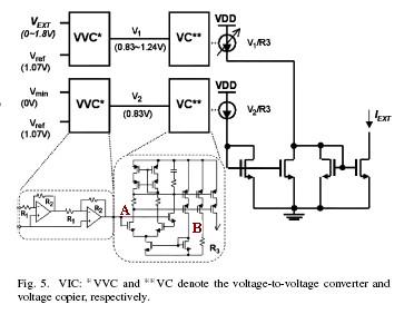
In the figure,VC** denotes the voltage copier and current generation。herei don't understand why VC** can copy voltage from node A to node B。
Could anybody explain it? thank you。
hi, wwm101
I suspect that the gate of the other NMOS of the differential pair should be connected to node "B". So the negative feedback loop will be established, and all things will make sense. Please think about it, thanx.
Thank you for your reply.
But how to explain the function of the NMOS whose gate is connected to node"A" and source is connected tothe gate of differential pair of the other NOMS at the right side?thank you.
wwm101 & waveguides:
Sorry to Mr. Waveguides, you are not totally right.
This NMOS is a Slew-Rate-enhancement element. In the case of node A is suddenly higher than node B by Vthn, this NMOS will be turned on very soon. At this transient, the gates of the current mirrors are pulled down, and node B is increased as a consequence.
From this analysis, we can find out that the differential mode input voltage of the differential pair will never be larger than Vthn, which makes the Opamp works in linear region all the time. Also, from this point of view, the NMOS' channel length will be the minimum length allowed in a given process, and its width will be as large as 100um, smaller or bigger, depending on the slew rate requirement.
wind2000sp3 &waveguides:
Thank you very much for your reply.
Here and now ,ican understand it.
wwm101,
Thank you too, for your interesting topics. There are so few topics discussing Linear Analog techniques in this forum, instead, almost all the members attach there reference in their topics. This job should be completed by a junior clerk, not an IC engineer.
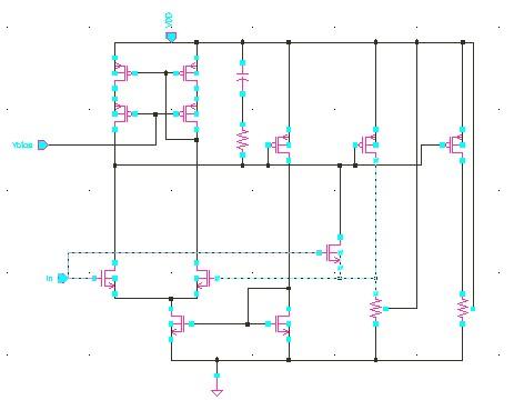
It can work when i connect the gate of the other NOMS of differential pairat the right side to the node 'B' .
The simulation resultwas shown inthe following.
But the result also shows that the NMOS doesn't enhance slew-rate significantly.
schematic

tran simulation result
thank you for your reply.
what kind of? Can you describe it to me ,please .thank you again.
不错不错
无条件支持!谢谢分享!97
really appreciated
wwm101,
The slew rate enhancement is a little tricky, whether it works well depends on the application evirement. For example, if you change the input pulse amplitude for 0.8V to 1.8V, I suspect the NMOS will work.
waveguides,
I'm also very interested in your solutions. It will be apreciated that if you share your ckt to us!
当不了沙泼还是要支持的!感谢感谢~
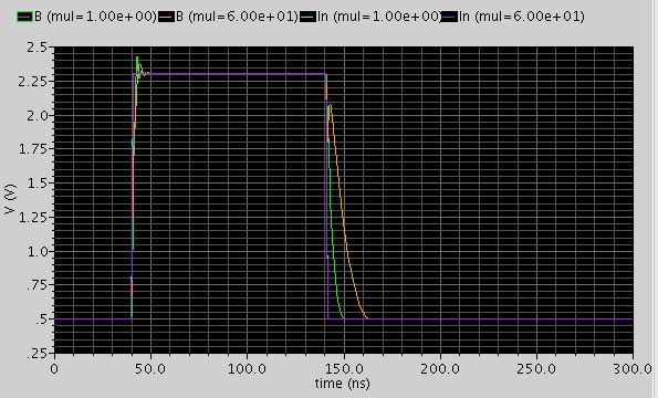
The tran simulation result is shown in the following figure after I set the input pwl amplitude for 0.5V to 2.3V.
In the figure,we can find thatthe simulation result is contrary to theoretical analysis .
the slew rate enhancement NMOS doesn't enhance slew rate but rather diminishs !howto explain it?thak you.
wwm101,
would you please tell us what process are you using? I find out that without the Nmos, the ckt's slew rate is about 1.8V/10nS, which is to the maximum limit of normal analog CMOS process. Thenthe Nmos will be useless.
dear wind2000sp3,
the design process is tsmc 0.18um rf process and the entire netlist is shown in the following .
// Library name: VGA
// Cell name: voltage-to-current-converter
// View name: schematic
R0 (net095 net78) resistor r=100
C1 (VDD net095) capacitor c=1p
R4 (net036 0 VDD) rppolywo_rf l=4u w=2u mf=(4)
R2 (B 0 VDD) rppolywo_rf l=6u w=2u mf=(1)
M13 (net35 net054 0 0) nmos_rf lr=400n wr=3u nr=5 m=1
M4 (net78 In net35 net35) nmos_rf lr=400n wr=3u nr=5 m=1
M5 (net092 B net35 net35) nmos_rf lr=400n wr=3u nr=5 m=1
M14 (net054 net054 0 0) nmos_rf lr=400n wr=3u nr=5 m=1
M12 (net78 In B B) nmos_rf lr=400n wr=3u nr=5 m=mul
M18 (net036 net78 VDD VDD) pmos_rf lr=400n wr=3u nr=5 m=30
M15 (net054 net78 VDD VDD) pmos_rf lr=400n wr=3u nr=5 m=4
M9 (B net78 VDD VDD) pmos_rf lr=400n wr=3u nr=5 m=30
M2 (net78 Vbias net69 net69) pmos_rf lr=400n wr=3u nr=5 m=1
M1 (net65 net092 VDD VDD) pmos_rf lr=400n wr=3u nr=5 m=1
M0 (net69 net092 VDD VDD) pmos_rf lr=400n wr=3u nr=5 m=1
M3 (net092 Vbias net65 net65) pmos_rf lr=400n wr=3u nr=5 m=1
wwm101,
Sorry I was busy in translating an article. From your infomation, I will suspect Vth=0.3V, a little more or less. Theorically speaking, the slew rate enhancement NMOS will work if your Opamp worked in turn-off region. There are two reasons:
1. The process element allows your Opamp's slew rate larger than 200V/uS, which is about 20 times of typically used analog process, whose minimum dimention is about 0.5~1um. In this case, the NMOS can be useless.
2. Otherwise, if the Opamp is turned off. All elements will stop to work, and so all parasitic caps are discharged. To turn the Opamp from off to on, the extra parasitic caps should be recharged, which contributes to an mount of delay time.
To verify my theory, you can apply a pulse, 0V to 1.5V, to the input of this ckt. I don't know what your simulator is, but in Hspice/Spectre, the option "UIC" should be "ON". B/c this option means whether you turn the parasitic caps on or off in transient analysis.
wind2000sp3,
thank you for your reminder,maybe i have found the reason why enhancement element can't indeed enhance the slew rate. that is because it was offset by its parasitic capacitances.
in thefigure 1,we can find the enhancement NMOS actually works to enhance the slew rate when input voltage value jumps up more then the VTH of NMOS,but its enhancement is offset by its parasitic GS cap.moreover its parasitic cap can further diminish the slew-rate when input voltage fall from high level to low,as shown in the fig2.
fig 1

fig2
In order to further verify my view,a capacitance was connect between the gate and source of enhancement NMOS. then we sweep the capacitance value by transient simulation and the result is shown in the following figure 3 &4.

fig3

fig4
So can we get a conlusion that the enhancement NMOS can't indeed enhance the slew rate because of its parasitic cap?
wwm101,
Now we are moving closer to the truth.
1. Your parasitic-cap theory can explain why the falling time is prolonged, that's what I mean or I want to mean;
2. But, the rising time can be enhanced indeed. My thoery is that if you apply 0~2V pulse, instead of 0.5V~2V pulse, to the circuit's input. In this case, all the mos FET are turned off, and all the parasitic should be charged. Then in the transient of input voltage rising from 0V to 2V, the Opamp is waking up, and this NMOS is responsible to accelarate the process of waking up the Opamp.
I recommend you to try it again, to apply 0V to 2V "pulse or pwl" waveform at the input. It may be interesting, or not at all. But I believe at least you wanna try to determine whether I'm right or wrong. I'm looking forward to your exciting result!
wind2000sp3,
Thank you for your patience reply.
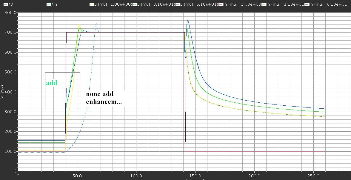
Today,I simulated the circuit with two different condition. One didn't add slew-rate enhancement element, the other one add slew-rate enhancement element.
And the transient simulation result was shown in the following.
In the figure,we can find that the enhancement NMOS can indeed enhance the SR of circuit.Butgreater width of NMOS doesn‘t indeed bringenhancement of SR because of its parasitic capacitance.
wwm101,
Congratulations to you!
wind2000sp3,
Thanks again
my two cents:
1) two wires missing in the original figure, one is for the self-biased cascode current mirror load
another is the feedback wire from B to negative input
2) this OpAmp use a self-biased scheme for its tail current source as well via feedback
3) nmos is rather a clamp instead of slew rate enhancer
