CC2530 功率输不出来
我司有用到CC2530,但是功率老是输不出来。测量CC2530差分输出仅有-30DBM,咋回事啊!
什么叫差分输出?你是怎么测的?用smartstudio+频谱仪吗?一般输出功率偏小跟阻抗不匹配有关,TI有提供参考设计
里面的readme.txt有对板材,厚度等的说明,请完全参照。射频部分的器件在*.xls文件中也有详细的参数,至少保证射频部分的器件
完全参照或接近。接着就是射频板设计要讲究的地方了,如下链接和说明
http://www.ti.com/general/docs/lit/getliterature.tsp?literatureNumber=swra367a&fileType=pdf
You can take a look at the readme.txt in the ref design. 4 layers .
Below is some additional notes when you are copying TI Reference design.
Understand the PCB board properties
– PCB stack-up
– PCB board dielectric properties (dielectric constant and loss tangent).
– TI reference designs include a document describing above properties Readme.txt
The checklist below provides important RF PCB design considerations to be followed
- Verify the stack-up matches the reference design. If the design is a 4-layer PCB; verify that ground plane is layer two right below top/component side.
- Changing the layer spacing/stack-up will affect the matching in the RF signal path and should be carefully accounted for as explained in AN068
- Ensure that you follow the datasheet layout recommendation unique to the part (CCXXXX).
- 0603(mills) discrete parts are not recommended because of size and parasitic values.
- Verify that bypassing/decoupling capacitors are as close as possible to the power supply pins that they are meant to bypass/decouple.
- Ensure each decoupling capacitor only decouples the specific pins recommended on the reference design and that the capacitor is correct value and type.
- Ensure that decoupling is done pin<>capacitor<>via.
- Verify that the ground plane matches the reference design. There should be a solid ground plane below the device and the RF path.
- Verify that RF signal path matches the reference design as closely as possible. Components should be arranged in a very similar way and oriented the same as the reference design.
- The crystal oscillator should be as close as possible to the oscillator pins of the part. Long lines to the oscillator should be avoided if possible.
- Verify that the top ground planes are stitched to the ground plane layer and bottom layer with many vias around the RF signal path. Compare to the reference design. Vias on the rest of the board should be no more than l/10 apart.
- If the part has differential output, ensure that the traces in the differential section and differential section are symmetrical as in the reference design.
- If the design uses a battery (such as a coin cell), the battery will act as a ground plane and should therefore not be placed under the antenna.
- If the reference design specifies using T-Lines (Transmission Lines), it is very critical to ensure that the T-Lines match the reference design exactly.
- Verify that the under-the-device power pad layout is correct. The solder pads and mask should match and the opening size should ensure correct amount of paste. Vias should be the correct number and masked/tented to ensure that they don’t suck up all the solder, leaving none to solder the chip to pad. (Refer to the datasheet for the recommended layout for the corresponding part)
- The board should specify impedance controlled traces. That is, the layer spacing and FR4 permittivity should be controlled and known.
Important considerations for Antennas
- If using an antenna from a TI reference design, be sure to copy the design exactly as drawn and check if the stack-up in the reference design matches your stack-up.
- Changes to feed line length of antenna will change input impedance match.
- PCB and chip antennas should not have any ground plane under them.
- Any metal in close proximity, plastic enclosure, and human body will change the antennas input impedance and resonance frequency, which must be considered in the design.
- For multiple antenna on same board, use antenna polarization and directivity to isolate.
- For chip antennas verify that the spacing from and orientation with respect to the ground plane is correct as specified in their datasheet.
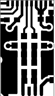
smartstudio+无线通信测试仪,四层板,图片见截图,
cc2591出来到天线,你做了些什么?我怎么看到一条弧线?你的天线是PCB的还是chip的。
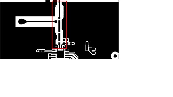
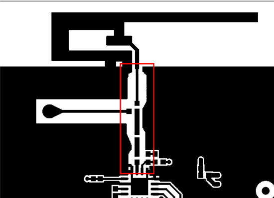
参考设计如下,红色框的线宽,线距等请严格遵循,否则需要自己去算阻抗匹配50欧姆。
用了CC2591,在smartstudio中有没有允许PA?
chip ANTA, PA为RF6505.PA工作使能OK,也工作起来啦,问题是你CC2530输出信号太弱啦,基本没输出
你好,根据参考设计的pcb,RF 线宽为13mil,但实际算出的线宽为11mil为50R,还有阻抗部分的走线为23mil,这样的设计是如何考虑的?
另外查分部分要不要也做阻抗控制?谢谢!