CC3200 ADC 采集错误
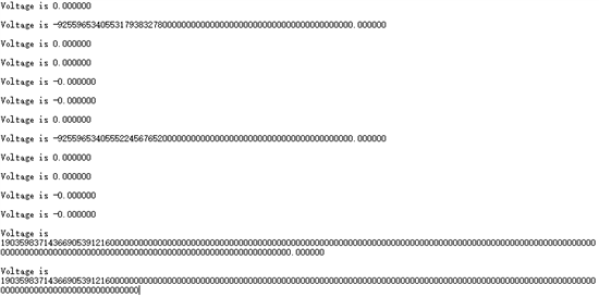
采用官方例程&LaunchXL,分别将PIN_58(ADC_CH1)接到GND和板子3.3v用3个10k电阻分压到1v左右,出现的结果如图1,2,请问是否是芯片的问题

图1,看接到GND上没问题

接到1v左右的电压上就飘了
本大师给你分析分析:
如果接到GND和VCC都是没问题的,那么问题就出在你的分压上了,你用了很大的电阻进行分压,接入ADC后,可知道ADC相当于引入一个电阻了呢?
如果想靠谱,分压后取电出,用跟随器缓冲一下。这个是常用的手法,防止因为阻抗问题导致测量不准。
另外你可以降低这个分压电阻的阻值试试看,应该会好很多。不过功耗就大了。
参考如下连接http://processors.wiki.ti.com/index.php/CC3200_ADC_Appnote
Battery voltage measurement
The most widely used case of the ADC is to measure the voltage of the battery to give an indication to the user, or to take some evasive action before shutdown. Since the input range of the ADC is limited to 1.4V max and the battery voltage can vary from 2.3V to 3.3V depending upon the battery type and age, some scaling of the signal is required. This scaling can easily be implemented using a resistive divider network. Let us assume that the max voltage = 3.3V. Then we can scale 3.3V using the scaling factor of 1.4V/3.3V.
Simple resistive divider (Not recommended)
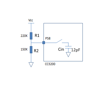
Let us consider the case where R1 = 220K and R2 = 150K as shown for the voltage divider in the figure below.

In the figure above, the switch represents the ADC sampling. While in the sampling phase, the switch will be closed for a duration of 400ns. During this phase the internal capacitor (12pF) gets charged from the external voltage divider.
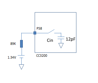
The thevenin's equivalent circuit for the external circuit is shown in the figure below.

Using the standard capacitor charging equation, we can calculate the voltage at the capacitor at the end of the sampling time (400ns)
Using Vc = V (1 - e^(-t/RC)), we get the final voltage on the capacitor at the end of 400ns as 0.42V.
Note that the error is very large in this measurement and this is not a good method of measurement. This error however can be overcome by adding a capacitor at the ADC pin as shown the following section.
Resistive divider with buffer capacitor (Recommended)

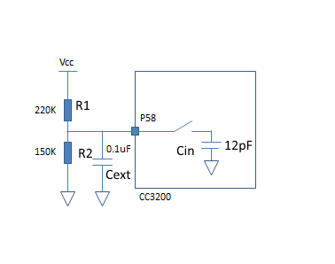
With the above circuit, the external capacitor gets charged to 1.34V through the resistor divider while the ADC is not connected to the pin. When the ADC is connected to the pin, the internal capacitor starts to charge from the external capacitor. Since the switch resistance is negligible and the external capacitor is quite large compared to the internal one, the 12pF cap can charge to the final value of 1.34V.
The external capacitor is calculated based on the following calculation. Assuming that the Cin is charged from Cext fully, this will result in a charge re-distribution. Assuming that the entire charge is supplied from the Cext, we should not let the Cext voltage drop below 1LSB of the ADC. So we can calculate
Cext = Cin x 4096 which gives 50nF. For margin we can assume 2x the calculated value and use 100nF (0.1uF).
Note that the use of the external capacitor restricts the measurement bandwidth. Neglecting the effect of Cin (too small comprated to Cext), the overall 3dB bandwidth is limited to 1/(2*pi* R*Cext) where R is the parallel combination of R1 and R2.
In this particular case, the bandwidth is 17.8 Hz, which is good enough to estimate battery voltage as it will smoothen down fast transients dips due to peak currents.
Further averaging has to be performed in software to get better estimate of the voltage.
