ADS8638数据输出问题
ADS8638根据手册上看写寄存器的时候,DOUT应该是0x0000的,但是为什么我写寄存器的时候,同时有数据输出?

以下是我的代码
#include "DSP2833x_Device.h"     // DSP2833x Headerfile Include File
#include "DSP2833x_Examples.h"   // DSP2833x Examples Include File
#include "SciSetup.h"

#define	  LedReg	(*((volatile  Uint16 *)0x41FF))
Uint16    *ExRamStart = (Uint16 *)0x100000;

void senddata(Uint16 a, int num);

#define ALPD GpioDataRegs.GPADAT.bit.GPIO26

// Prototype statements for functions found within this file.
// interrupt void ISRTimer2(void);
void delay_loop(void);
void spi_xmit(Uint16 a);
void spi_fifo_init(void);
void spi_init(void);
void error(void);
unsigned int Spi_TxReady(void);
unsigned int Spi_RxReady(void);

void main(void)
{
   Uint16 sdata;  // send data
   Uint16 rdata;  // received data

// Step 1. Initialize System Control:
// PLL, WatchDog, enable Peripheral Clocks
// This example function is found in the DSP2833x_SysCtrl.c file.
   InitSysCtrl();

// Step 2. Initalize GPIO:
// This example function is found in the DSP2833x_Gpio.c file and
// illustrates how to set the GPIO to it's default state.
// InitGpio();  // Skipped for this example
// Setup only the GP I/O only for SPI-A functionality
// This function is found in DSP2833x_Spi.c

   InitXintf16Gpio();	//zq

   InitSpiaGpio();

   EALLOW;
      GpioCtrlRegs.GPAMUX2.bit.GPIO26 = 0;
      GpioCtrlRegs.GPAPUD.bit.GPIO26=0;
      GpioCtrlRegs.GPADIR.bit.GPIO26 = 1;
      EDIS;

// Step 3. Clear all interrupts and initialize PIE vector table:
// Disable CPU interrupts
   DINT;

// Initialize PIE control registers to their default state.
// The default state is all PIE interrupts disabled and flags
// are cleared.
// This function is found in the DSP2833x_PieCtrl.c file.
   InitPieCtrl();

// Disable CPU interrupts and clear all CPU interrupt flags:
   IER = 0x0000;
   IFR = 0x0000;

// Initialize the PIE vector table with pointers to the shell Interrupt
// Service Routines (ISR).
// This will populate the entire table, even if the interrupt
// is not used in this example.  This is useful for debug purposes.
// The shell ISR routines are found in DSP2833x_DefaultIsr.c.
// This function is found in DSP2833x_PieVect.c.
   InitPieVectTable();

// Step 4. Initialize all the Device Peripherals:
// This function is found in DSP2833x_InitPeripherals.c
// InitPeripherals(); // Not required for this example
   spi_fifo_init();	  // Initialize the Spi FIFO
   spi_init();		  // init SPI


// Step 5. User specific code:
// Interrupts are not used in this example.
	LedReg = 0xFF;


		ALPD=1;		  //PowerUP
//	 	spi_xmit(0x080E);//PowerDown
//		spi_xmit(0x0800);//PowerUp

     for(;;)
      {
        // Transmit data
    	 spi_xmit(0x0201);//自动采集

      }

}


// Step 7. Insert all local Interrupt Service Routines (ISRs) and functions here:

void delay_loop()
{
    long      i;
    for (i = 0; i < 1000000; i++) {}
}


void spi_init()
{
	SpiaRegs.SPICCR.all =0x000F;	             // Reset on, falling edge, 16-bit char bits
	SpiaRegs.SPICTL.all =0x0006;    		     // Enable master mode, normal phase,
                                                 // enable talk, and SPI int disabled.
	SpiaRegs.SPIBRR =0x00FF;
	SpiaRegs.SPICCR.all =0x008F; 		// relinquish SPI from reset

    SpiaRegs.SPIPRI.bit.FREE = 1;                // Set so breakpoints don't disturb xmission
}

void spi_xmit(Uint16 a)
{

	Uint16 rdata1;  // received data
	if(Spi_TxReady() == 1)
	{
		SpiaRegs.SPITXBUF=a;
	}
	while(Spi_TxReady() != 1)
	{

	}

	if(Spi_RxReady() == 1)
	{
	   rdata1 = SpiaRegs.SPIRXBUF;
	 }

	delay_loop();
}

void spi_fifo_init()
{
// Initialize SPI FIFO registers
    SpiaRegs.SPIFFTX.all=0xA040;
    SpiaRegs.SPIFFRX.all=0x204f;
    SpiaRegs.SPIFFCT.all=0x0;
}

unsigned int Spi_TxReady(void)	//发送就绪
{

	unsigned int i = 0;
	if(SpiaRegs.SPISTS.bit.BUFFULL_FLAG == 1)
{
	i = 0;
}
else
{
	i = 1;
}
	return (i);
}

unsigned int Spi_RxReady(void)	//接收就绪
{

	unsigned int i = 0;
	if(SpiaRegs.SPISTS.bit.INT_FLAG == 1)
{
	i = 0;
}
else
{
	i = 1;
}
	return (i);
}


//===========================================================================
// No more.
//===========================================================================
sh手册讲是 Invalid data 并没有说是 Zero. 你可以忽略, 不去在意具体数值
但是我采集数据或者读寄存器的时候也无法得到正确的值,比如我先写复位,然后读复位寄存器,发现结果不对。

我的AL_PD是使用PowerDown功能,在开始发送数据之前我先把这个引脚设置为高电平,然后发送设置复位寄存器的指令(0X0201),然后读复位寄存器(0X0300),结果接收的值不对,低8位本来应该是0000 0001,但是现在确是0011 1100 ,不知道是不是我前面哪里还需要什么参数设置之类的问题?或者是我发送数据的方式不对吗?
SPI频率是多少?
发送数据的时序: 7bit register address+R/W+8bit data
谢谢您的回答。
SpiaRegs.SPIBRR =0x007F; //SPI波特率=37.5M/128=293kHZ;
SPI的波特率大概是293kHZ,发送数据的时序是按照那样发送的。
我想请问手册里写的PowerUp和PowerDown是否需要另外设置?是否有简单的自测方式可以测试芯片是否正常工作?
谢谢!
而且芯片只通+-15V电源时很烫,但是加上3.3V的AVDD和DVDD之后,芯片就冷下来了,不知道这个情况是否正常?
AVDD的电压范围为4.75V~5.25V,所以AVDD的最小电压为4.75V, DVDD给3.3V没问题。YuTing Chen
而且芯片只通+-15V电源时很烫,但是加上3.3V的AVDD和DVDD之后,芯片就冷下来了,不知道这个情况是否正常?
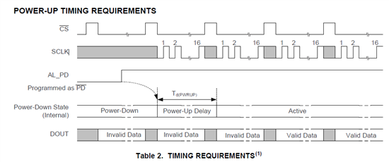
把AL_PD配置为power down功能的话,那么上电过程AL_PD pin是一个由低到高的过程,您看下上电时序,如下图:
另外,是否方便将SPI clock提高到1MHz试试再验证下?您参考下这个帖子:
https://e2e.ti.com/support/data_converters/precision_data_converters/f/73/p/324021/1128546?tisearch=e2e-quicksearch&keymatch=ADS8638%20%20register#1128546
谢谢您的回答。
我情况跟链接里面的这个类似,但是我把频率增加到1M甚至更高的时候,还是不行。
我看手册上写AL_PD默认的是作为PD模式的,也就是输入模式,我使用的时候把这个脚接到GPIO的一个引脚上,然后使用程序把其拉到高电平,这种方法正确不?还是直接把它接到3.3V上?
还有,写配置寄存器之前除了发送复位的指令(即配置01h的寄存器),还需要进行什么初始化的操作吗?
谢谢!
我把AVDD 和DVDD都接到5V的电源就可以正常工作了