TLK10022评估板配置
您好:
我购买了TLK10022评估板,想将一路5Gbps数据分成四路,现不接信号时就有四路数据输出,接上信号后输出数据码型没有变化,这是什么原因?
正常工作时需要通过GUI来做配置的。配置芯片的速率,serdes工作模式。。。。。
网上应该可以下载到GUI guideline:
TLK10022 and TLK10081 Multi-Rate Lane Aggregator
Evaluation Module (EVM) Graphical Users Interface (GUI)
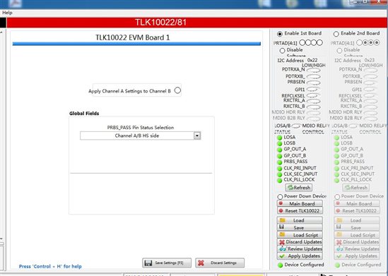
我是使用GUI来控制的,我现在是外部输入5G数据,输入一个125M参考时钟,可是输出数据不对,请问该如何配置。
Device Pins Settings
- Ensure PDTRXA_N pin is high (Power Down disabled)
- Ensure REFCLK_SEL pin is low
- Ensure PRBSEN pin is low (Pattern Generation disabled)
GLOBAL_CONTROL_1
Write 0x8610 to 0x00 //Perform a global reset or assert RESET_N pin
CHANNEL_CONTROL_1
Write 0x4004 to 0x01// Link Training Enabled, TX_1LN_MODE_SEL enabled (1 lane in transmit datapath)
HS_SERDES_CONTROL_1
Write 0x831D to 0x02 // Ultra high bandwidth, PLL in HS Serdes Enabled, HS_PLL_MULT 20x
HS_SERDES_CONTROL_2
Write 0xA848 to 0x03 // Depending of every system AC losses, length of traces or cables, is needed to adjust some parameter of this register such as HS_SWING, HS_AGCCTRL, etc.
HS_SERDES_CONTROL_3
Write 0x1500 to 0x04 // Evenly that Register 0x03 is needed to adjust some parameters of this register to tune the device according to the system. Refer to tables in datasheet to select the correct settings for some parameters of equalization
HS_SERDES_CONTROL_4
Write 0x2000 to 0x05 // Adjust some parameters to tune the device (Pre, Main and post cursor)
LS_SERDES_CONTROL_1
Write 0x8115 to 0x06 // If user needs to configure an specific lane is needed to modify GLOBAL_LN_WRITE & LS_LN_CFG_EN
LS_SERDES_CONTROL_2
Write 0xDE06 to 0x07 // Quarter Rate for 1.25Gbps in the low speed side, please refer to datasheet for more settings. Also, adjust parameters for Low Speed Side (Swing, LOS, De-enphasis, etc)
LS_SERDES_cONTROL3
Write 0x000D to 0x08 // Low speed side equalization control and polarity control
HS_OVERLAY_CONTROL
Write 0x0380 to 0x09 // LOS pin reflection
LS_TP_OVERLAY_CONTROL
Write 0x0500 to 0x0A// Oversampling in LS path, test pattern generation and verification, delay in transmitter of LS, etc.
HS_TP_CONTROL
Write 0x0520 to 0x0B // Test Pattern Generation, vertification and remote loopback.
CLK_SEL_CONTROL
Write 0x0000 to 0x0D
RESET_CONTROL
Write 0x0008 to 0x0E // Perform a datapath reset once the desired configuration is set
配置不出来我想要的结果,试了一个月了。
我没有配置过这款芯片,不过你对着“”TLK10022 and TLK10081 Multi-Rate Lane Aggregator
Evaluation Module (EVM) Graphical Users Interface (GUI)“ 这个指导操作,检查下每个步骤和寄存器的状态是否正常,应该可以得到你要的记过。
”TLK10022 and TLK10081 Multi-Rate Lane Aggregator
Evaluation Module (EVM) Graphical Users Interface (GUI)“
这个说明书里并没有介绍如何配置,只说了大概的功能,配置上没有讲,请问有相关的技术支持么?
非常感谢!