关于ADS1118的SPI通信问题以及读取数据问题
亲们~大家好,我最近在使用一款模数转换芯片ADS1118,现在遇到以下问题,希望可以得到大家的帮助,小弟感激不尽~~
1.ADS1118和单片机(我用的是MSP430F149)通信要使用SPI通信协议,但我现在不清楚如何读取模数转换之后的数字量,比如说怎么使用SPI中断读取数据?仅仅只用在中断函数体中写 “Data = U0RXBUF” 吗?
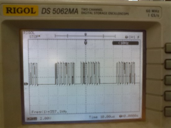
2.单片机执行程序之后与ADS1118进行通信之后,我在SCLK引脚上检测到了时钟信号,与TI提供的说明书上的波形基本一样,(波形图如下)不知道正不正确,请大家帮忙看看~~
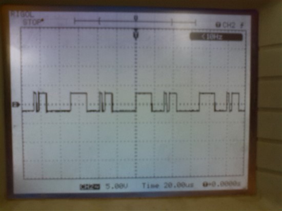
3.但检测 ADS1118 的 DOUT 引脚时却出现这样的波形,不论有没有模拟量输入都是的波形,如下图,这我就费解了...
最后我的硬件连接图如下:
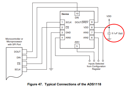 我将AIN0接正电压,AIN1接地这个连接方式有错误吗?
程序如下(我用的是默认配置,没有修改):(我使用的是IAR Embedded Workbench进行编程的)
#include <msp430x14x.h>
#define CPU_F ((double)8000000)
#define delay_us(x) __delay_cycles((long)(CPU_F*(double)x/1000000.0))
#define delay_ms(x) __delay_cycles((long)(CPU_F*(double)x/1000.0))
#define uchar unsigned char
#define uint unsigned int
#define CS_L P2OUT = 0X00
#define CS_H P2OUT = 0Xff
#define LED_ON P1OUT = 0xff
#define LED_OFF P1OUT = 0x00
char cmd[] = {0x05,0xeb,0x00,0x00},SLV_Data = 0xFF;
uint a = 0,U0TX_BYTE=1;
void SPI_WRITE()
{
uint i;
CS_L;
//while(!U0TX_BYTE);
for(i=0;i<4;i++)
{
TXBUF0 = cmd[i]; // Transmit first character
//while(!U0TX_BYTE);
//U0TX_BYTE = 0;
}
CS_H;
}
int main(void)
{
unsigned int i;
WDTCTL = WDTPW + WDTHOLD; // Stop WDT
P1OUT = 0x000; // Setup P1.0 for LED output
P1DIR |= 0x0ff;
P2DIR |= 0X0FF;
P3SEL = 0x00E; // Setup P3 for SPI mode
P3OUT = 0x020; // Setup P3.4 for Scope trigger and
P3DIR |= 0x030; // P3.5 for slave initialization
U0CTL = CHAR + SYNC + MM + SWRST; // 8-bit, SPI, Master
U0TCTL = SSEL1 + STC; // SMCLK, 3-wire
U0BR0 = 0x002; // SPICLK = SMCLK/2
U0BR1 = 0x000;
U0MCTL = 0x000;
ME1 = USPIE0; // Module enable
U0CTL &= ~SWRST; // SPI enable
IE1 |= URXIE0; // Recieve interrupt enable
_EINT(); // Enable interrupts
P3OUT &= ~0x020; // Toggle P3.5: slave reset
P3OUT |= 0x020;
i = 50000; // Delay
do (i--);
while (i != 0);
CS_L;
while (1)
{
CS_L;
//SPI_WRITE(); // Transmit first character
while ((IFG1 & UTXIFG0) == 0);
TXBUF0 = 0x05; //给ADS1118发送数据
TXBUF0 = 0x8B;
TXBUF0 = 0x00;
TXBUF0 = 0x00;
CS_H;
LPM0; // CPU off
//while(1);
}
} // End Main
#pragma vector = USART0RX_VECTOR
__interrupt void SPI0_rx (void)
{
CS_L;
P1OUT = U0RXBUF;
//P3OUT ^= 0x010; // XOR P3.4 for scope trigger
while ((IFG1 & UTXIFG0) == 0); // USART0 TX buffer ready?
//P1OUT = 0XFF;
TXBUF0 = 0x05;
TXBUF0 = 0xeb;
TXBUF0 = 0x00;
TXBUF0 = 0x00;
CS_H;
}
恳请大家提供帮助与建议,不胜感激,跪谢Orz
你好,
SPI的主设备(单片机)如果不发送数据的话,是不会有clock信号的,所以读取转换结果的时候,可以在单片机端发送0X00或0XFF,这样可以为ADS1118输出数据提供clock信号,不会改变ADS1118的配置寄存器(跟NOP1/0位有关,详见数据手册22页)。单片机端发送0X00或0XFF后,ADS1118返回的数据将会进入RXBUF,如果你的程序是采用SPI中断读取数据的话,那么在中断函数里面写“Data = U0RXBUF” 可以读到转换结果或配置寄存器的值。
数据读取的时序可以参考数据手册23页DATA RETRIEVAL章节。你可以将你写入的配置寄存器值读出,校验一下是否正确,这可以顺便确认一下通信时序是否正确。
能否将SPI的SCLK , SDO, SDI, CS这几个引脚的时序在示波器上同时抓出来?单独一个引脚的时序难于分析。
AIN0接正电压,AIN1接地这个连接方式是否合理需要根据配置寄存器里面的MUX[2:0], PGA[2:0]这几个位而定,你的正电压是给的是多少V?
首先十分感谢Martin先生的热心帮助,现在情况是这样的,我更换了主控制器,现在使用的是Launchpad msp430G2553,也换了ADS1118,SPI的SCLK , SDO, SDI, CS这几个引脚的时序如下:
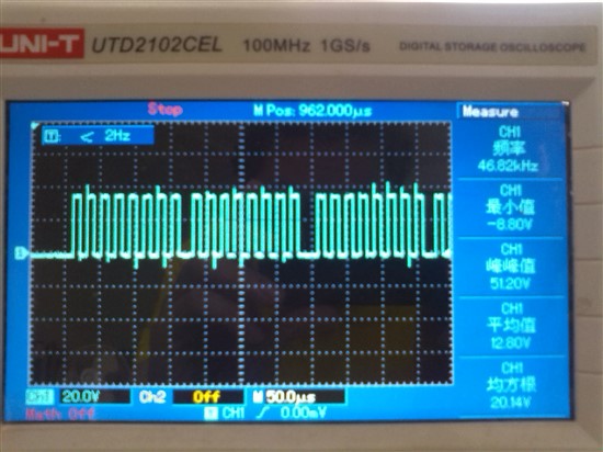
图1 SCLK时序图
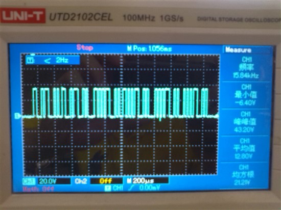
图2 SDO时序图
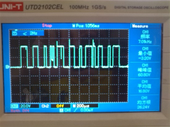
图3 SDI时序图
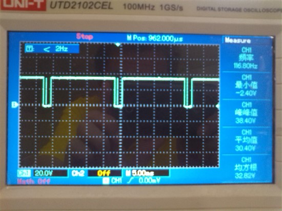
图4 CS时序图
在抓出的这4幅图里面,我发现 SDI 的波形有些奇怪,我配置的 MUX[2:0] = 100 即 AINP = AIN0,AINN is GND;PGA[2:0] = 010 即 FS = 正负2.048V,在实际硬件连接里我 AIN0 接 +3.5V,那按此配置的话,应该从ADS1118接收到的数据是7FFFH才对啊,那为什么会出现 SDI 那样的波形?
我的程序如下:(由于使用的是TI工程师给的G2553与ADS1118的模块程序,有些不懂的地方已用红字写出,还望指教~~)
#include <msp430g2553.h>
/*
* ======== Grace related includes ========
*/
//#include <ti/mcu/msp430/csl/CSL.h>
/*
* ======== Function Calls ========
*/
void uart_txc(char c);
void uart_txstr(char *c);
/* "hex2asc" Converts a 32-bit integer n into an ASCII string.
digs is the maximum number of digits to display. Conversion is controlled
by mode, as follows:
- mode = 0: Leading zeroes are not printed. The string may be
less than digs digits long.
- mode = 1: Spaces are printed in place of leading zeroes. The
string will be digs digits long.
- mode = 2: Leading zeroes are printed. The string will be digs
digits long.
If the number is zero, at least one zero is printed in all modes.
This routine works by converting n to an 8-byte BCD number and calling
hex2asc. No division by 10 is performed.
*/
int hex2asc(void *n, int digs, int mode, char *s);
void ADS_Config(void);
void ADS_Read(int data[]);
void Send_Result(int *data);
void Port_Config(void);
signed int WriteSPI(unsigned int config, int mode);
void delay(void);
#define h2a(d) ((d>9)?(d+'A'-10):(d+'0'))
#define LITTLEENDIAN 1
/*
* ======== main ========
*/
int main(int argc, char *argv[])
{
int i = 0;
CSL_init(); // Activate Grace-generated configuration
// >>>>> Fill-in user code here <<<<<
// Initialize TC data array
signed int data[6];
// Port configuration
Port_Config();
// Set ADS1118 configuration
ADS_Config();
while (1)
{
// Read the data from both input pairs
ADS_Read(data);
// Transmit the data out the UART
Send_Result(data);
P1OUT = (data[0] >> (i))& 0x0001;
i++;
if(i == 16) i = 0;
}
return (0);
}
void Port_Config(void)
{
// Set P1.0, P1.3, P1.4, P2.1, P2.2, P2.4, P2.5, P2.6 and P2.7 low
P1OUT = 0x00;
P2OUT = 0x01 ;
}
/*
* Initial configuration routine. A header file could be created, but the configuration is really rather simple.
* In this case a 16-bit value representing the register contents is set to variable temp
*/
void ADS_Config(void)
{
int i;
unsigned int temp;
// Set the configuration to AIN0/AIN1, FS=+/-1.024, SS, DR=128sps, PULLUP on DOUT
//temp = 0x78A;
temp = 0x458A;
// Set CS low and write configuration
P2OUT &= ~BIT0;
// Write the configuration
WriteSPI(temp,0);
// Set CS high to end transaction
P2OUT |= BIT0;
}
void ADS_Read(int data[])
{
unsigned int j, temp;
// Set the configuration to AIN0/AIN1, FS=+/-1.024, SS, DR=128sps, PULLUP on DOUT
//temp = 0x78A;
temp = 0x458A;
// Set CS low and write configuration
P2OUT &= ~BIT0;
// First the data is captured by writing to each device to take start a conversion for A0-A1
WriteSPI(temp,1);
// Set CS high to end transaction
P2OUT |= BIT0;
/*
* Now we pause slightly before reading the data, or it is possible to either poll the DOUT/DRDY or enable an interrupt
* where the DOUT/DRDY transition from high to low triggers a read. In this case it is kept quite simple with a delay
*/
delay(); // May be needed depending on method
// When we read the data we restart the conversion with new mux channel A1 (此处不明白为什么要重新选择另外一个通道开启转换,难道不能只对一个通道的电压值进行转换吗?本函数以下的语句可以去掉吗?)
//temp = 0x378A;
temp = 0x558A;
// Set CS low and write configuration
P2OUT &= ~BIT0;
// Read the earlier conversion result and set to the new configuration
data[0] = WriteSPI(temp,1);
delay(); // May be needed depending on method
// Read second channel data
data[1]=WriteSPI(temp,0);
// Set CS high to end transaction
P2OUT |= BIT0;
}
signed int WriteSPI(unsigned int config, int mode)
{
signed int msb;
unsigned int temp;
char dummy;
temp = config;
if (mode==1) temp = config | 0x8000; // if mode is set to 1, this command should initiate a conversion
/*
* The process of communication chosen is to always send the configuration and read it back
* this results in a four byte transaction. The configuration is 16-bit (or 2 bytes) and is transmitted twice.
*
*/
while(!(UC0IFG&UCB0TXIFG)); // Make sure buffer is clear
/*
* First time configuration is written
*/
UCB0TXBUF = (temp >> 8 ); // Write MSB of Config
while(!(UC0IFG&UCB0RXIFG));
msb=UCB0RXBUF; // Read MSB of Result
while(!(UC0IFG&UCB0TXIFG));
UCB0TXBUF= (temp & 0xff); // Write LSB of Config
while(!(UC0IFG&UCB0RXIFG));
msb = (msb << 8) | UCB0RXBUF ; //Read LSB of Result
/*
* Second time configuration is written, although data could be sent as NOP in either transmission, just simplified in this case
*/
while(!(UC0IFG&UCB0TXIFG));
UCB0TXBUF = (temp >> 8 ); // Write MSB of Config
while(!(UC0IFG&UCB0RXIFG));
dummy=UCB0RXBUF; // Read MSB of Config
/*
* One advantage of reading the config data is that DOUT/DRDY is forced high which makes it possible to either poll the state or set an interrupt
*/
while(!(UC0IFG&UCB0TXIFG));
UCB0TXBUF= (temp & 0xff); // Write LSB of Config
while(!(UC0IFG&UCB0RXIFG));
dummy=UCB0RXBUF; //Read LSB of Config
return msb;
}
/*
* Following code relates to formatting the data for transmission on UART
*/
void Send_Result(int *data)
{
unsigned int i;
int intval = 0;
char char_array[5];
// Poke out data
uart_txstr("TEMPS:");
uart_txc('\r');
uart_txc('\n');
for (i=0; i<2; i++)
{
intval = data[i];
hex2asc(&intval, 4, 2, char_array);
uart_txstr(char_array);
uart_txc('\r');
uart_txc('\n');
}
}
int hex2asc(void *npos, int digs, int mode, char *s)
{
int i,zero;
char dig;
char *spos=s;
char *n=(char *)npos;
zero=1;
#if LITTLEENDIAN
n+=(digs-1)>>1;
#else
n+=(16-digs)>>1;
#endif
for (i=digs-1;i>=0;--i) {
if (i&1) {
dig=(*(char *)n>>4)&15;
} else {
dig=*(char *)n&15;
#if LITTLEENDIAN
--n;
#else
++n;
#endif
}
if (zero&&dig)
zero=0;
if (zero) {
switch(mode) {
case 1:
*spos++=' ';
break;
case 2:
*spos++='0';
break;
default:
break;
}
} else
*spos++=h2a(dig);
}
if (zero&&mode==1)
*(spos-1)='0';
else if (zero&&mode==0)
*spos++='0';
*spos=0;
return spos-s;
}
void uart_txc(char c)
{
while (!((UC0IFG&UCA0TXIFG)));
UCA0TXBUF=c;
}
void uart_txstr(char *c)
{
while (*c) uart_txc(*(c++));
}
void delay(void)
{
unsigned int k;
for (k = 8000; k = 0; k--) __no_operation();
}
你现在这个好使了吗?我也用的是149.好用的话能不能发一份给我。行不。邮箱1003287885@qq.com
149的好使了吗?可以发我一份吗?谢谢!540362098@qq.com
149好了吗?能发我一份吗?非常感谢!501883466@qq.com