ADS1251问题
时间:10-02
整理:3721RD
点击:
ADS1251的DOUT引脚,开始是有波形,但是度数却全部为1,后来波形都没有了,一直为高,求解答!
Hi
首先确认一下供电,再确认时序。
The result of the A/D conversion is written to the DOR from the Most Significant Bit (MSB) to the Least Significant Bit (LSB) in the time defined by t1 (see Figures 11 and 12). The DOUT/DRDY line then pulses LOW for the time defined by t2 , and then drives the line HIGH for the time defined by t3 to indicate that new data are available to be read. At this point, the function of the DOUT/DRDY pin changes to DOUT mode. Data are shifted out on the pin after t7 .
t1,t2,t7的 DOUT/DRDY可以正常测量到吧?

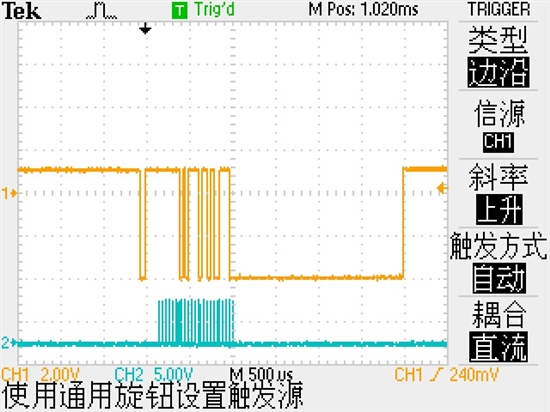
DOUT和CLK的波形。

DOUT和SCLK的波形。
给的差分输入电压都大于0V
可以侧量出来。

给的电压为0V的时候居然有数据。并且数据不稳定。
输入为0v的时候居然有数据,且数据部稳定
您好,我是电子新手,我想把ADS1251与DSP2809通讯,怎么连接端口?求告知