关于LMP91300 的 SWIF编程烧写寄存器的电平问题.
请教 Martin:
在LMP91300的数据手册里有以下这段:
Single-Wire Interface (SWIF)
The LMP91300 uses a bi-directional Single Wire Interface protocol to program and read registers. To
communicate with the LMP91300 (slave) through the SWIF interface, the micro controller (master) must transmit
(write) data through the DC loop supply voltage that should be set to +8V during programming or communication.
This superimposed signal of pulses transitions between 8V and 12V is on top of the +8V DC loop supply voltage.
When the master transmits data into the LMP91300 the signal propagates into the SENSE2+ pin through the
supply. The master receives data from the LMP91300 through the LED pin in the form of alternating current
pulses. These current pulses will be 5mA in amplitude. The LED pin must be connected to ground, either through
an LED or directly connected to ground for the LMP91300 to talk to the master.
能详细解释一下吗?
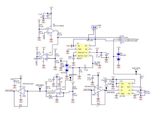
我已按下面图做出好编程器.但不明白供电电压8V和12V分别在何时提供?
请求指点.
the micro controller (master) must transmit (write) data through the DC loop supply voltage that should be set to +8V during programming or communication
整个数据传输过程中, DC loop 电源应该提供 8V。
This superimposed signal of pulses transitions between 8V and 12V is on top of the +8V DC loop supply voltage.
传输的信号应该在 8V 之上,8V 或者 12V (我觉得这应该是指高低电平,根据上下文再确认一下吧)。
下文如下:
没有提及8V或12V.能否理解为.数据信号的高电平为12V.低电平为8V呢?
但是从LMP91300SWIFEVM User’s Guide的电路原理图看,并非如此.而且是控制电源回路在8V或12V,不是控制数据信号8V或12V,.数据信号高电平为12V.低电平为0V.这是怎么解释呢?
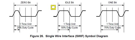
The communication scheme utilizes various pulse width waveforms to represent different symbols as shown in
Figure 26. The binary representation of a zero bit is represented by a 25% pulse duty cycle, a one bit is
represented by a 75% pulse duty cycle, and idle bit is represented by a 50% duty cycle. All pulses transmitted
must fall within the pulse width specifications provided within the electrical characteristics table.
Figure 26. Single Wire Interface (SWIF) Symbol Diagram
The LMP91300 can be programmed at an input transfer bit rate between 1kbps to 10kbps. There is no
acknowledge signal during the input data transfer so the master should read back the data to ensure data
integrity and a successful data transfer has occurred. A read transaction is executed by the master transmitting
data to configure the pointer register resulting in data output transfer by the slave. The LMP91300 transmits read
back data at a speed of about 7kbps.