ADS1282寄存器读写完全正常,但是转换数据全为0,寄存器需要如何设置
如图,采用的是连续读数模式,电路连接图完全按照如下连接
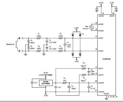
供电DVDD=+3.3V, AVDD/AVSS=±2.5V, VREFP/VREFN=±2.5V,CLK为2.048MHz有源晶振SYNC/nPWDN/nRESET均上拉,未用的M0/M1/MCLK均下拉,
请求指点
请检查按照手册24页的相关要求进行操作,
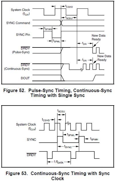
In Continuous-sync mode, either a single sync pulse
or a continuous clock may be applied. When a single
sync pulse is applied (rising edge), the device
behaves similar to the Pulse-sync mode. However, in
this mode, DRDY continues to toggle unaffected but
the DOUT output is held low until data are ready, 63
DRDY periods later. When the conversion data are
non-zero, new conversion data are ready (as shown
in Figure 52)
When a continuous clock is applied to the SYNC pin,
the period must be an integral multiple of the output
data rate or the device re-synchronizes. Note that
synchronization results in the restarting of the digital
filter and an interruption of 63 readings (refer to
Table 10).
When the sync input is first applied, the device
re-synchronizes (under the condition tSYNC ≠ N/fDATA).
DRDY continues to output but DOUT is held low until
the new data are ready. Then, if SYNC is applied
again and the period matches an integral multiple of
the output data rate, the device freely runs without re-synchronization
我还是有点不太明白,就是说我直接把SYNC脚拉高是不对的,应该用MCU控制此管脚,我这样理解对吗?
然后,如果我想工作在CONTINUOUS-SYNC的模式下,当DRDY变低,然后送32个SCLK,然后给SYNC管脚送1US的脉冲(此时DRDY已经变高),依次循环下去,这样的思路对吗?
但是按照这样的思路,DRDY就没有低电平了。。。
是不是我得按照
这个图片的时序编写命令?
感谢您的回答。
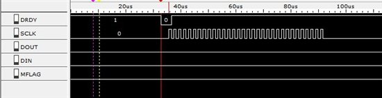
对不起,我的DOUT脚没连到逻辑分析仪上,在原来简单的连接方法上测试了一下输入短接的数据,如下
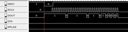
但是数据明显不对,我的SYNC直接拉高了,请教是什么问题。。。
是不是得按照您说的24页来设置?还是?
目前所有寄存器全部使用的默认值,除了给ADS1282发送了一个RESET命令外,其余都没有发送,请问
大概会是什么问题?
感谢您的回答!