OPA1632的第7脚问题
OPA1632的第7脚的作用是什么?
按照数据表的说明:
7.4.1 Shutdown Function
The shutdown (enable) function of the OPA1632 is referenced to the negative supply of the operational amplifier.
A valid logic low (< 0.8 V above negative supply) applied to the enable pin (pin 7) disables the amplifier output.
Voltages applied to pin 7 that are greater than 2 V above the negative supply place the amplifier output in an
active state, and the device is enabled. If pin 7 is left disconnected, an internal pull-up resistor enables the
device. Turn-on and turn-off times are approximately 2 μs each.
Quiescent current is reduced to approximately 0.85 mA when the amplifier is disabled. When disabled, the output
stage is not in a high-impedance state. Thus, the shutdown function cannot be used to create a multiplexed
switching function in series with multiple amplifiers.
我理解为当第7脚电压<0.8V时是禁止放大器输出的,因此如此设计一款电路:
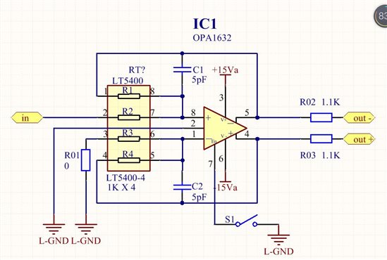
OPA1632的第7脚连接一个开关(S1)到地,作为静音开关。
但实际使用中S1的开关对1632没有任何作用,实测S1开时第7脚14.94V、S1闭合时第7脚0V,在这两种状态下1632的输入、输出波形没有任何变化,是何原因?
您的理解是正确的。第7脚enable的threshold电压:
Enable:>(V-)+2V
Disable:<(V-)+0.8V.
也就是说,比如单电源供电,当Pin7电压小于0.8V时,为低电平,OPA1632 输出disable。当电压大于2V时,为高电平,输出enable。
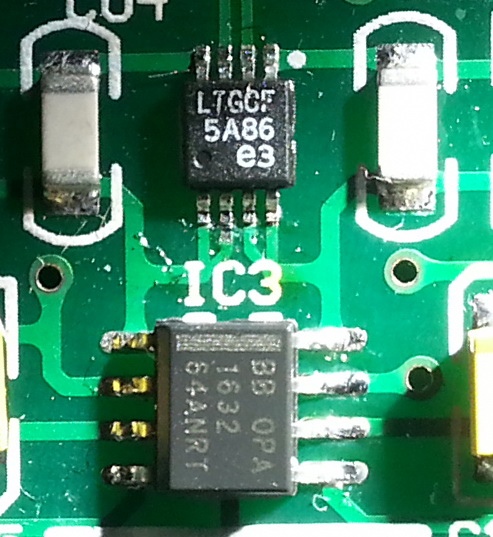
但从板子上来看,芯片表面是BB公司的logo,不是TI的logo呢?
感谢您的回复。
那么在双电源供电的情况下,如何有效使用第7脚呢?
另外,BB不是早就被Ti收购了吗?
双电源供电同样啊,高低电平的threshold电平还是:
Enable:>(V-)+2V
Disable:<(V-)+0.8V.
BB是被TI收购了,但是收购之后OPA1632芯片的表面打印应该是TI的logo。所以按照你的描述,7脚disable和enable时仍有输出,怀疑是芯片自身问题。
感谢您的指导,芯片没有问题,以前我的理解有偏差:认为Disable:<0.8V,也就是对地电压小于0.8V,应该是Disable:<(V-)+0.8V,现在已经验证:把第7脚接到V-,Disable功能正常了。