tas5630在PBTL模式下 接通电源就处于关断模式
tas5630在PBTL模式下 接通电源就处于关断模式,芯片不工作,但是能够测得VREG是3.7v的电压,芯片各个管脚的电压都正常。请问这是为什么啊?一直查不出是什么原因。芯片接通电源后,sd是亮的,otw接通瞬间亮了一下。芯片的out-A测量对地短路。
Hi, Weizhi,
Can you send more information about the failure.
-What is the power supply?
-what is the input signal(Vrms and frequency)?
-what is the load?
If you can send out the circuit, I think it will be more quickly to find the issue.
Best Regards.
PVDD采用的是50v,芯片的是12v,
 这个是主芯片的电路图,采用pbtl电路,信号还没有加进去,只是刚通电就显示shutdown状态,附件中是整个设计电路。麻烦您查看一下,谢谢
Hi,Weizhi,
The sch. looks fine.
Shutdown occurs due to a wide range of fault conditions, such as UnderVolatage, OverLoad, OverTemp or Pin to Pin Short Circuit (PPSC) protection.
So, I have another two questions:
1. What's the resistance of the load?
2.How do you deal with the heatsink?
Best regards.
1.If running with an open load, the LC filter might not have enough dampening. During transients or square waves on the inputs, oscillations can occur in the LC filter which can cause damage to the IC.
2.Grounding the heatsink is vital. It is very important to follow the rules about PCB layout shown in the data sheet and the EVM PCB layout.
负载的电阻是10欧姆,散热采用cpu散热方式,散热片加风扇,散热片对地接触良好,请问芯片正常工作时,芯片的输出是否对地短路,例如我的pcb版中out-a是对地短路的。
It is abnormal that the out_a pin short to the GND. Please try another new chip.
Most inportant, make sure the voltage of the input not exceed 5V.
.
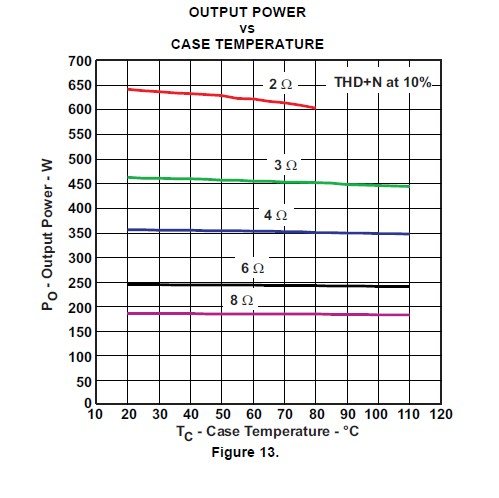 你好,我想问一下,pbtl模式下这张功率的图在两欧姆负载的情况下,为什么在温度超过80度以后就没有曲线图啦,还有就是输入线号的幅度不能超过5v,是tas5630的输入信号,还是opa1632的输入信号,这个输入信号不超过5v,是峰峰值,还是最大值。图中的功率是平均功率还是峰值功率?谢谢


这张功率的图在两欧姆负载的情况下,为什么在温度超过80度以后就没有曲线图啦,这张功率的图在两欧姆负载的情况下,为什么在温度超过80度以后就没有曲线图啦
Officially, TI does not guarantee ANY device specs or even device operation outside of the noted operating temperature range (0-70°C).
For figure 13, we didn't test the output power with 2Ω load when case temperature is above 80 ℃.
我们使用没发现问题,电感用的不对吧。注意驱动电压12-14v比较好用。