
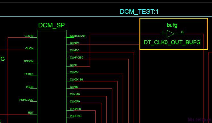
单单写了一个PLL_SP,综合是可以的,但是map时候报错了
时间:12-26
整理:3721RD
点击:
ERRORlace:1205 - This design contains a global buffer instance,
<DT_CLK0_OUT_BUFG>, driving the net, <DT_CLK0_OUT_BUFG>, that is driving the
following (first 30) non-clock load pins off chip.
< PIN: DT_CLK0_OUT1.O; >
This design practice, in Spartan-6, can lead to an unroutable situation due
to limitations in the global routing. If the design does route there may be
excessive delay or skew on this net. It is recommended to use a Clock
Forwarding technique to create a reliable and repeatable low skew solution:
instantiate an ODDR2 component; tie the .D0 pin to Logic1; tie the .D1 pin to
Logic0; tie the clock net to be forwarded to .C0; tie the inverted clock to
.C1. If you wish to override this recommendation, you may use the
CLOCK_DEDICATED_ROUTE constraint (given below) in the .ucf file to demote
this message to a WARNING and allow your design to continue. Although the net
may still not route, you will be able to analyze the failure in FPGA_Editor.
< PIN "DT_CLK0_OUT_BUFG.O" CLOCK_DEDICATED_ROUTE = FALSE; >
查了一下,好像是经过bufg的时钟不能直接输到IO口,要先经过ODDR2,请问这个ODDR2是什么,应该不是内存里面讲的DDR2,DDR3吧。
PIN "DT_CLK0_OUT_BUFG.O" CLOCK_DEDICATED_ROUTE = FALSE;
这句添加到UCF文件里面去。
我试了一下,在bufg后面添加一个ODDR2是可以解决问题的
- 加入Chipscope的CDC文件后,MAP报错,求指导!(1970-01-01)
- 请教:map后仿真是不是要加上GSR信号(1970-01-01)
- Example ofsynchronizationthrough binarysemaphore(1970-01-01)
- 关于FPGA实现过程mapping的问题!(1970-01-01)
- ise map出错(1970-01-01)
- ISE map中的错误(1970-01-01)
栏目分类
射频专业培训教程推荐