ads2013原理图直接转layout版图之后的端口设置问题
时间:03-15
整理:3721RD
点击:
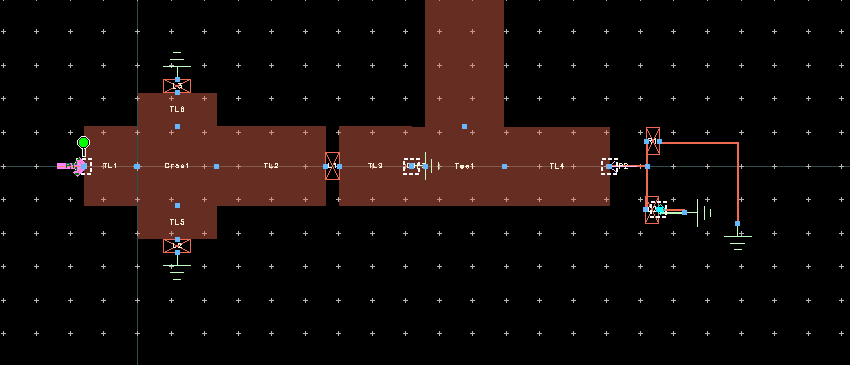
我做的一个微带线整流电路原理图想直接转为版图,请问port怎么加呢?
我直接加在两端会像下面这样报错
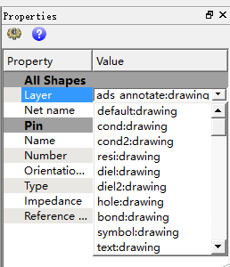
There are no layout pins on layers mapped in the substrate
P111 is on layer ( Layer Name = ads_annotate, Layer Num = 237) which is not mapped in the substrate
P22:P2 is on layer ( Layer Name = bound, Layer Num = 13) which is not mapped in the substrate
好像是说port没有在底板上映射? 本人新手求教怎么设置?
微带线图如下,谢谢


