silvaco tcad 沟槽功率MOS求助
时间:03-15
整理:3721RD
点击:
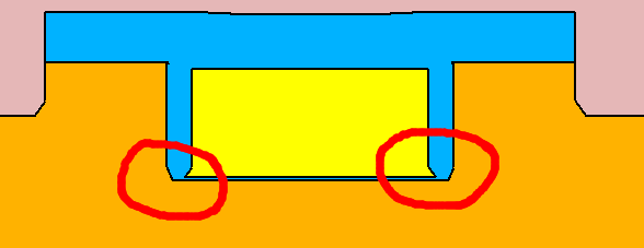
下面是我的工艺过程,我刻蚀沟槽的时候直接用的ETCH而不是etch rate,怎么我的管子出来成了这样
#
line x loc=0.00 spac=0.08
line x loc=0.20 spac=0.05
line x loc=0.40 spac=0.01
line x loc=0.60 spac=0.01
line x loc=0.75 spac=0.01
#
line y loc=0.00 spac=0.01
line y loc=1.00 spac=0.03
line y loc=2.00 spac=0.06
line y loc=3.00 spac=0.08
line y loc=4.00 spac=0.10
line y loc=5.00 spac=0.15
# sub define
init silicon c.arsenic=5e19 orientation=100 two.d
# create sub
etch silicon above p1.y=4
#epi1
deposit silicon thick=1.00 c.arsenic=1.12e15
#epi2
deposit silicon thick=1.00 c.arsenic=1.12e15
#epi3
deposit silicon thick=1.00 c.arsenic=1.12e15
#epi4
deposit silicon thick=1.00 c.arsenic=1.12e15
# trench etch
etch silicon start x=0.50 y=-0.01
etch cont x=0.50 y=1.50
etch cont x=0.75 y=1.50
etch done x=0.75 y=0.00
# annealing
diffus time=2 temp=950 nitro press=1.00
# gate oxidation
diffus time=10 temp=950 dryo2 press=1.00 hcl.pc=3
# gate oxidation
diffus time=10 temp=950 dryo2 press=1.00 hcl.pc=3
# gate oxidation
diffus time=10 temp=950 dryo2 press=1.00 hcl.pc=3
# gate oxidation
diffus time=10 temp=950 dryo2 press=1.00 hcl.pc=3
# gate oxidation
diffus time=10 temp=950 dryo2 press=1.00 hcl.pc=3
# gate oxidation
diffus time=10 temp=950 dryo2 press=1.00 hcl.pc=3
# gate oxide deposit
deposit oxide thick=0.0006 divisions=17
# polysilicon deposit
deposit polysilicon thick=0.93 c.phosphor=1.0e11 divisions=10
# etch polysilicon
etch polysilicon above p1.y=0.1
# etch oxide
etch oxide above p1.y=0.0
# oxide deposit
deposit oxide thick=1.00 divisions=10
# oxide deposit
deposit oxide thick=1.00 divisions=10
# oxide etch
etch oxide left p1.x=0.360
# p-body
implant boron dose=3e13 energy=400 tilt=7 rotation=28 crystal
# oxide etch
etch oxide above p1.y=0.05
# oxide deposit
deposit oxide thick=1.00 divisions=10
# oxide etch
etch oxide start x=0.23 y=-1.00
etch cont x=0.23 y=0.03
etch cont x=0.43 y=0.03
etch done x=0.43 y=-1.00
# n+
implant arsenic dose=1.2e14 energy=350 tilt=7 rotation=28 crystal
# annealing
diffus time=3 temp=950 nitro press=1.00
# oxide etch
etch oxide above p1.y=0.05
# pbody etch
etch silicon start x=0.00 y=0.00
etch cont x=0.00 y=0.70
etch cont x=0.25 y=0.70
etch done x=0.25 y=-0.01
# oxide deposit
deposit oxide thick=1.00 divisions=10
# 0xide etch
etch oxide left p1.x=0.23
# p+
implant boron dose=1e14 energy=100 tilt=7 rotation=28 crystal
# annealing
diffus time=3 temp=950 nitro press=1.00
# 0xide etch
etch oxide above p1.y=0.05
# oxide etch
etch oxide left p1.x=0.25
# bpsg deposit
deposit oxide thick=0.65 c.arsenic=1.0e11 c.boron=1.0e11 divisions=10
# bpsg etch
etch oxide left p1.x=0.25
# aluminum deposit
deposit aluminum thick=0.35 divisions=10
#
struct mirror right
#
electrode name=source x=0.40 y=0.15
#
electrode name=source x=1.10 y=0.15
#
electrode name=gate x=0.75 y=0.90
#
electrode name=drAIn backside
#
line x loc=0.00 spac=0.08
line x loc=0.20 spac=0.05
line x loc=0.40 spac=0.01
line x loc=0.60 spac=0.01
line x loc=0.75 spac=0.01
#
line y loc=0.00 spac=0.01
line y loc=1.00 spac=0.03
line y loc=2.00 spac=0.06
line y loc=3.00 spac=0.08
line y loc=4.00 spac=0.10
line y loc=5.00 spac=0.15
# sub define
init silicon c.arsenic=5e19 orientation=100 two.d
# create sub
etch silicon above p1.y=4
#epi1
deposit silicon thick=1.00 c.arsenic=1.12e15
#epi2
deposit silicon thick=1.00 c.arsenic=1.12e15
#epi3
deposit silicon thick=1.00 c.arsenic=1.12e15
#epi4
deposit silicon thick=1.00 c.arsenic=1.12e15
# trench etch
etch silicon start x=0.50 y=-0.01
etch cont x=0.50 y=1.50
etch cont x=0.75 y=1.50
etch done x=0.75 y=0.00
# annealing
diffus time=2 temp=950 nitro press=1.00
# gate oxidation
diffus time=10 temp=950 dryo2 press=1.00 hcl.pc=3
# gate oxidation
diffus time=10 temp=950 dryo2 press=1.00 hcl.pc=3
# gate oxidation
diffus time=10 temp=950 dryo2 press=1.00 hcl.pc=3
# gate oxidation
diffus time=10 temp=950 dryo2 press=1.00 hcl.pc=3
# gate oxidation
diffus time=10 temp=950 dryo2 press=1.00 hcl.pc=3
# gate oxidation
diffus time=10 temp=950 dryo2 press=1.00 hcl.pc=3
# gate oxide deposit
deposit oxide thick=0.0006 divisions=17
# polysilicon deposit
deposit polysilicon thick=0.93 c.phosphor=1.0e11 divisions=10
# etch polysilicon
etch polysilicon above p1.y=0.1
# etch oxide
etch oxide above p1.y=0.0
# oxide deposit
deposit oxide thick=1.00 divisions=10
# oxide deposit
deposit oxide thick=1.00 divisions=10
# oxide etch
etch oxide left p1.x=0.360
# p-body
implant boron dose=3e13 energy=400 tilt=7 rotation=28 crystal
# oxide etch
etch oxide above p1.y=0.05
# oxide deposit
deposit oxide thick=1.00 divisions=10
# oxide etch
etch oxide start x=0.23 y=-1.00
etch cont x=0.23 y=0.03
etch cont x=0.43 y=0.03
etch done x=0.43 y=-1.00
# n+
implant arsenic dose=1.2e14 energy=350 tilt=7 rotation=28 crystal
# annealing
diffus time=3 temp=950 nitro press=1.00
# oxide etch
etch oxide above p1.y=0.05
# pbody etch
etch silicon start x=0.00 y=0.00
etch cont x=0.00 y=0.70
etch cont x=0.25 y=0.70
etch done x=0.25 y=-0.01
# oxide deposit
deposit oxide thick=1.00 divisions=10
# 0xide etch
etch oxide left p1.x=0.23
# p+
implant boron dose=1e14 energy=100 tilt=7 rotation=28 crystal
# annealing
diffus time=3 temp=950 nitro press=1.00
# 0xide etch
etch oxide above p1.y=0.05
# oxide etch
etch oxide left p1.x=0.25
# bpsg deposit
deposit oxide thick=0.65 c.arsenic=1.0e11 c.boron=1.0e11 divisions=10
# bpsg etch
etch oxide left p1.x=0.25
# aluminum deposit
deposit aluminum thick=0.35 divisions=10
#
struct mirror right
#
electrode name=source x=0.40 y=0.15
#
electrode name=source x=1.10 y=0.15
#
electrode name=gate x=0.75 y=0.90
#
electrode name=drAIn backside
some one upload tutorial
http://bbs.eetop.cn/thread-380063-1-1.html